

InAs quantum dot-based remote epitaxial structure, preparation method and application
An epitaxial structure and quantum dot technology, which is applied in the fields of final product manufacturing, sustainable manufacturing/processing, photovoltaic power generation, etc., can solve the problem of reducing battery short-circuit current and photoelectric conversion efficiency, low size and position distribution uniformity, and affecting quantum dot crystals. Quality and other issues, to achieve the effect of alleviating large tearing, reducing defect density, and inhibiting structural dissimilation
- Summary
- Abstract
- Description
- Claims
- Application Information
AI Technical Summary
Problems solved by technology
Method used
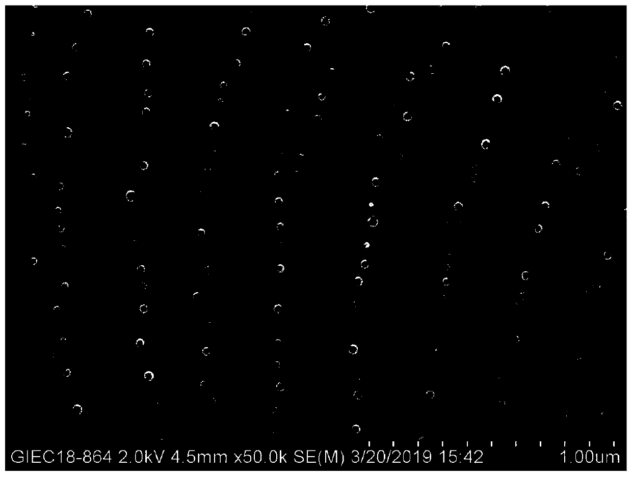
Image

Examples
Embodiment 1
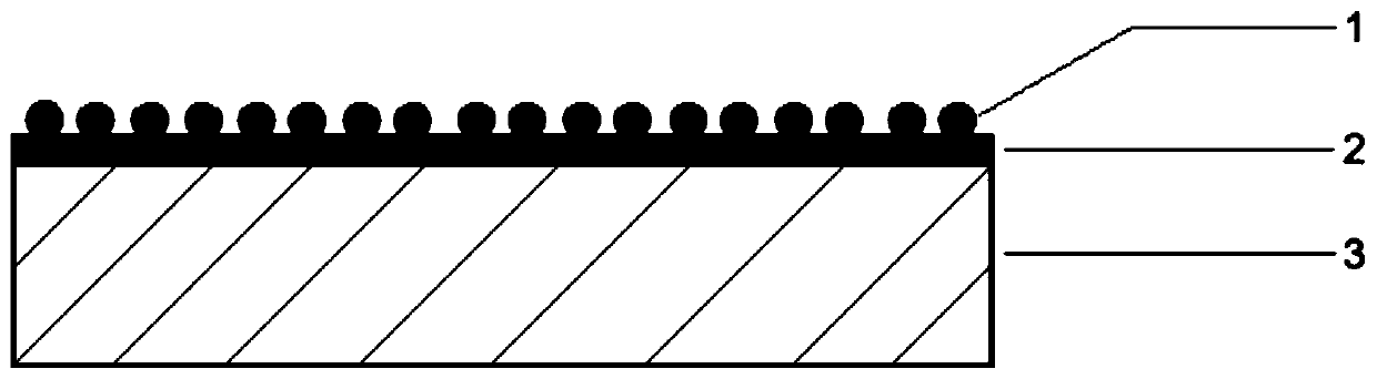
[0031] (1) The highly doped n-type GaAs substrate is used as the base material, the crystal orientation is (100), and the Si doping concentration is 5.1×10 18 / cm 3 , the carrier mobility is 1336cm 2 / (vs.). In order, ultrasonic cleaning was performed with AR grade acetone, ethanol and ultrapure water for 5 minutes, followed by rinsing with 6% hydrochloric acid for 3 minutes, and then rinsing with deionized water.
[0032] (2) Graphene transfer: Graphene is a single-layer graphene grown on a copper base, and the preparation method is a conventional CVD method (refer to Dervishi E, Li Z, Watanabe F, et al.Large-scale graphene production by RF-cCVD method[J].Chemical Communications, 2009(27):4061.), before transferring, graphene needs to be transferred to ferric chloride solution of 1mol / L, after the copper metal substrate is completely dissolved, use PMMA accompanying sheet to transfer graphite The alkene was transferred in ultrapure water three times, each time for 3 minute...
Embodiment 2
[0038] (1) Using a highly doped n-type GaAs substrate as the base material, the crystal orientation is (001), and the Si doping concentration is 5.1×10 19 / cm 3 , the carrier mobility is 1600cm 2 / (vs.). In order, ultrasonic cleaning was performed with AR grade acetone, ethanol and ultrapure water for 5 minutes, followed by rinsing with 6% hydrochloric acid for 3 minutes, and then rinsing with deionized water.
[0039] (2) Graphene transfer: Graphene is a single-layer graphene grown on a copper base, and the preparation method is a conventional CVD method (refer to Dervishi E, Li Z, Watanabe F, et al.Large-scale graphene production by RF-cCVD method[J].Chemical Communications, 2009(27):4061.), before transferring, graphene needs to be transferred to ferric chloride solution of 1mol / L, after the copper metal substrate is completely dissolved, use PMMA accompanying sheet to transfer graphite The alkene was transferred in ultrapure water three times, each time for 3 minutes, t...
PUM
| Property | Measurement | Unit |
|---|---|---|
| Concentration | aaaaa | aaaaa |
Abstract
Description
Claims
Application Information