A kind of electronic nose device and preparation method thereof
An electronic nose and device technology, applied in the field of electronic nose devices and their preparation, can solve the problems that electronic nose devices cannot meet the requirements of distributed sensing, achieve selectivity and difference, and overcome the effect of high working temperature
- Summary
- Abstract
- Description
- Claims
- Application Information
AI Technical Summary
Problems solved by technology
Method used
Image
Examples
preparation example Construction
[0047] The present invention also provides a preparation method for the above-mentioned electronic nose device, comprising the following steps:
[0048] S1. Forming a patterned FET-type metal electrode array on the substrate.
[0049] Process the metal electrode array pattern on the substrate through photoresist, and then deposit the metal electrode on the substrate by evaporation, sputtering, ion plating, laser pulse or molecular beam epitaxy. The specific steps are as follows:
[0050] S1.1, first use negative photoresist to perform first photolithography on a clean substrate to form M gate patterns;
[0051] S1.2. Using any method of evaporation, sputtering, ion plating, laser pulse or molecular beam epitaxy, metal electrodes are deposited on the substrate described in step S1.1, so that the gate pattern area forms a gate Pole 2;
[0052] S1.3, using the shadow mask metal mask as a mask, depositing a metal oxide on the metal electrode layer described in step S1.2 to form ...
Embodiment 1
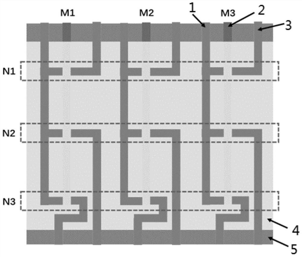
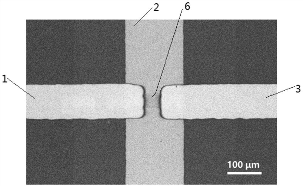
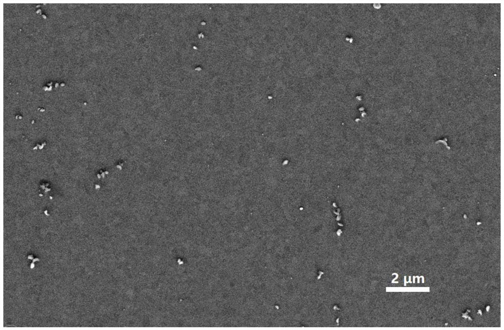
[0068] refer to figure 1 , an electronic nose device, the substrate is a silicon oxide wafer, a layer of back gate is sputtered on the substrate first, and then Al 2 o 3 The dielectric layer, and finally the source and drain electrodes are sputtered, and the electrodes are in a 3×3 array. Graphene was grown by CVD, and the graphene was wet-transferred to the conductive channel region, and the conductive channel pattern was etched by oxygen plasma. The channel length was 70 μm and the width was 50 μm. Sputtering of TiO on the conductive channel of row N1 of the sensor array 2 Nanoparticles, N2 row evaporated SiO 2 Nanoparticles, row N3 is unmodified. During the gas sensing test, the grid voltage applied to the M1 column of the sensor array is -5V, the M2 column grid voltage is 0V, and the M3 column grid voltage is 5V.
[0069] Figure 4 is the response of the three conductive channels above column M2 of the sensor array to 100ppm methane, ethane, propane, ethanol, acetone...
PUM
 Abstract
Description
Claims
Application Information


