Anode modification method of perovskite solar cell
A solar cell and anode modification technology, applied in the direction of circuits, photovoltaic power generation, electrical components, etc., can solve the problems of blocked lateral transport of carriers, reduced battery output power, and reduced short-circuit current, so as to improve photoelectric conversion efficiency and improve device performance. Stability, effect of increasing current and voltage
- Summary
- Abstract
- Description
- Claims
- Application Information
AI Technical Summary
Problems solved by technology
Method used
Image

Examples
Embodiment 1
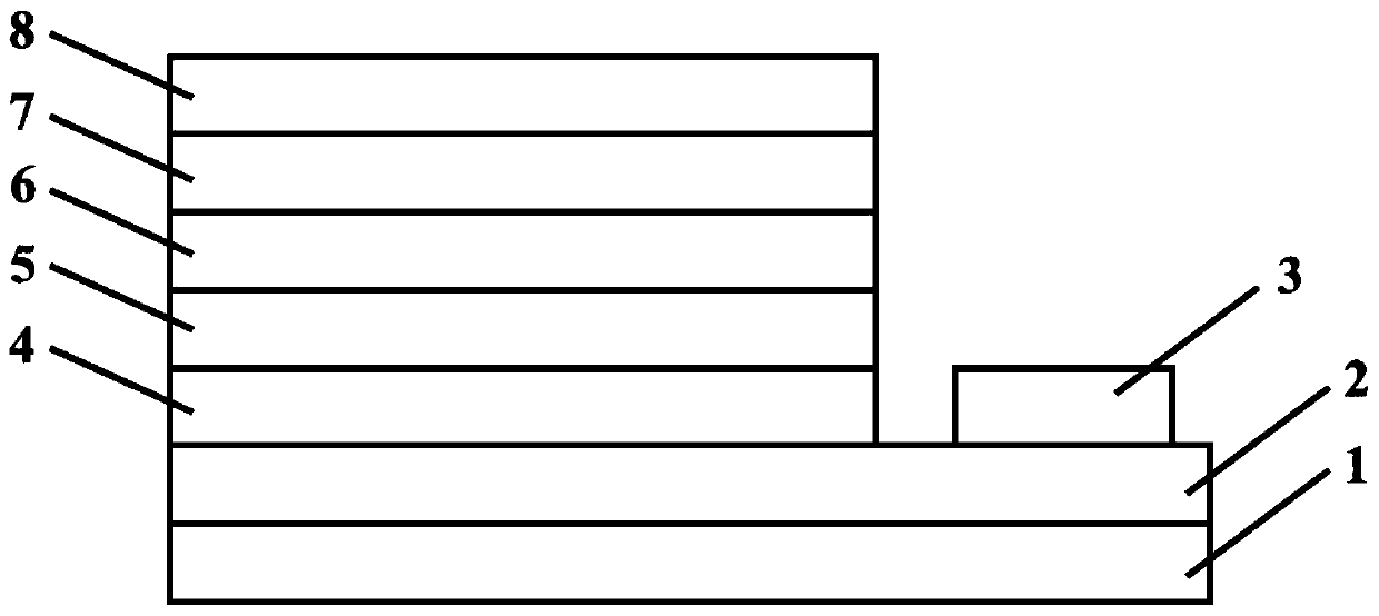
[0036]1) Prepare an electron transport layer (TiO 2 , SnO 2 , ZnO, PCBM, C 60 , Nb 2 o 5 , SrTiO 3 , ICBA, ICTA), thickness of 50 ~ 1500nm perovskite film (ABX 3 , where A is MA (methylamine), FA (formamidine), 5-AVA (5-ammonium isovalerate) or C S and combinations thereof, B is Cu, Ni, Fe, Co, Mn, Cr, Cd, Sn, Pb, Pd, Ge, Eu or Yb and combinations thereof, X is I, Br or Cl or combinations thereof), the thickness is 1~ 300nm hole transport layer (spiro-OMeTAD, NiO x , CuI, CuSCN, NiO x , PEDOT:PSS, CuCSN, Graphene oxide, Cu 2 O, CuO, CuCaO 2 , P3HT, VO x ).
[0037] 2) On the battery that has prepared the hole transport layer, use a vacuum thermal evaporation coating machine with multiple evaporation sources to prepare the halide modification layer and the metal silver electrode. The halide evaporation source is a single halide powder with a purity higher than 99% or blocks. Before starting evaporation, the chamber vacuum is lower than 6×10 -4 Pa, adjust the curre...
Embodiment 2
[0039] 1) Prepare an electron transport layer (TiO 2 , SnO 2 , ZnO, PCBM, C 60 , Nb 2 o 5 , SrTiO 3 , ICBA, ICTA), thickness of 50 ~ 1500nm perovskite film (ABX 3 , where A is MA (methylamine), FA (formamidine), 5-AVA (5-ammonium isovalerate) or C S and combinations thereof, B is Cu, Ni, Fe, Co, Mn, Cr, Cd, Sn, Pb, Pd, Ge, Eu or Yb and combinations thereof, X is I, Br or Cl or combinations thereof), the thickness is 1~ 300nm hole transport layer (spiro-OMeTAD, NiO x , CuI, CuSCN, NiO x , PEDOT:PSS, CuCSN, Graphene oxide, Cu 2 O, CuO, CuCaO 2 , P3HT, VO x ).
[0040] 2) Use a vacuum thermal evaporation coating machine with multiple evaporation sources to prepare a halide modification layer and a metal silver electrode on the battery that has prepared a hole transport layer. The halide evaporation source is two or more halides with a purity higher than 99%. Mixed powder or block. Before starting evaporation, the chamber vacuum is lower than 6×10 -4 Pa, adjust the c...
Embodiment 3
[0042] 1) Prepare an electron transport layer (TiO 2 , SnO 2 , ZnO, PCBM, C 60 , Nb 2 o 5 , SrTiO 3 , ICBA, ICTA), thickness of 50 ~ 1500nm perovskite film (ABX 3 , where A is MA (methylamine), FA (formamidine), 5-AVA (5-ammonium isovalerate) or C S and combinations thereof, B is Cu, Ni, Fe, Co, Mn, Cr, Cd, Sn, Pb, Pd, Ge, Eu or Yb and combinations thereof, X is I, Br or Cl or combinations thereof), the thickness is 1~ 300nm hole transport layer (spiro-OMeTAD, NiO x , CuI, CuSCN, NiO x , PEDOT:PSS, CuCSN, Graphene oxide, Cu 2 O, CuO, CuCaO 2 , P3HT, VO x ).
[0043] 2) Use a vacuum thermal evaporation coating machine with multiple evaporation sources to prepare a halide modification layer and a metal silver electrode on the battery that has prepared a hole transport layer. The halide evaporation source is two or more halides with a purity higher than 99%. The powder or block of the substance is placed in two or more heating boats respectively. Before starting evap...
PUM
| Property | Measurement | Unit |
|---|---|---|
| Thickness | aaaaa | aaaaa |
| Thickness | aaaaa | aaaaa |
| Thickness | aaaaa | aaaaa |
Abstract
Description
Claims
Application Information
 - R&D
- Intellectual Property
- Life Sciences
- Materials
- Tech Scout
- Unparalleled Data Quality
- Higher Quality Content
- 60% Fewer Hallucinations
Browse by: Latest US Patents, China's latest patents, Technical Efficacy Thesaurus, Application Domain, Technology Topic, Popular Technical Reports.
© 2025 PatSnap. All rights reserved.Legal|Privacy policy|Modern Slavery Act Transparency Statement|Sitemap|About US| Contact US: help@patsnap.com