an inducement (sb 4 se 6 ) n Preparation method of antimony selenide photoelectric thin film with longitudinal growth of molecular chain

A vertical growth, photoelectric thin film technology, applied in circuits, electrical components, semiconductor devices, etc., can solve the problems of narrow process window, unsuitable for industrial production, etc., to achieve high application value, low cost, simple and practical effect of preparation process

Active Publication Date: 2022-08-05
NORTHEAST DIANLI UNIVERSITY
View PDF11 Cites 0 Cited by
  • Summary
  • Abstract
  • Description
  • Claims
  • Application Information

AI Technical Summary

Problems solved by technology

The prior art generally obtains vertically grown (Sb 4 Se 6 ) n Molecular chains, but this method has a narrow process window and is not suitable for industrial production

Method used


Image

  • an inducement (sb  <sub>4</sub> se  <sub>6</sub> )  <sub>n</sub> Preparation method of antimony selenide photoelectric thin film with longitudinal growth of molecular chain
  • an inducement (sb  <sub>4</sub> se  <sub>6</sub> )  <sub>n</sub> Preparation method of antimony selenide photoelectric thin film with longitudinal growth of molecular chain
  • an inducement (sb  <sub>4</sub> se  <sub>6</sub> )  <sub>n</sub> Preparation method of antimony selenide photoelectric thin film with longitudinal growth of molecular chain

Examples


preparation example Construction

[0019] The one-step method refers to doping during the preparation of the substrate film, and the method used may be low pressure chemical vapor deposition technology, thermal evaporation technology, magnetron sputtering technology, ultrasonic spray technology or spin coating technology.

[0020] The two-step method refers to doping by post-treatment after the substrate film is prepared, and the adopted method may be ultrasonic spray technology or spin coating technology, and then the doping process is completed by annealing treatment.

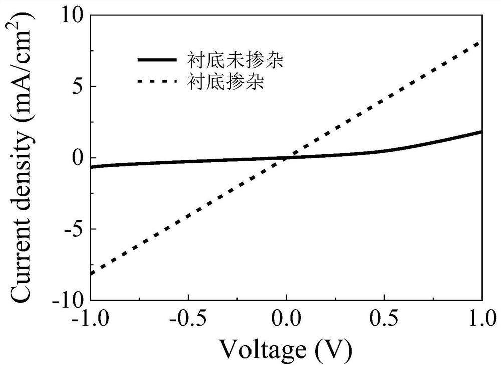
[0021] prepared (Sb 4 Se 6 ) n Antimony selenide photoelectric thin films grown longitudinally by molecular chains can be used to fabricate antimony selenide photoelectric devices, such as solar cells or photodetectors.

[0022] Antimony selenide optoelectronic device structure can be glass / transparent conductive film / electron transport layer / antimony selenide / hole transport layer / metal electrode, glass / transparent conductive film / hole trans...

Embodiment 1

[0023] Example 1: Preparation of antimony selenide photoelectric thin film by one-step method:

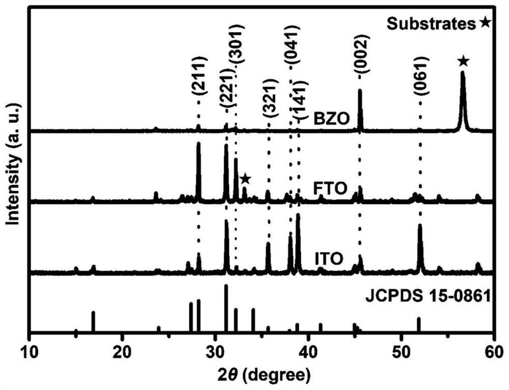
[0024] (1) ZnO thin films were prepared by low-pressure chemical vapor deposition technology, in which the flow rates of diethylzinc and water were 300 sccm and 350 sccm, respectively, and hydrogen-diluted borane (B 2 H 6 ) as the doping source, the flow rate is 150sccm, the deposition temperature is 200°C, the deposition pressure is 150 Pa, and the deposition time is 800s to form a boron-doped zinc oxide (BZO) substrate film;

[0025](2) The antimony selenide film was prepared on the BZO substrate film by the rapid thermal evaporation method, the vacuum degree was 5Pa; the substrate film temperature was 300°C; the evaporation source temperature was 450°C; the evaporation time was 90s, and the thickness was 1000 nm. The antimony selenide light absorbing layer;

[0026] (3) On the antimony selenide layer, spin-coating a PEDOT:PSS film at 2500 rpm for 60 s to prepare a hole transpo...

Embodiment 2

[0030] Example 2: Preparation of antimony selenide photoelectric thin film by two-step method:

[0031] (1) Soak the FTO conductive glass with detergent, acetone, isopropanol, ethanol and deionized water for 30 minutes in sequence, and then blow dry with nitrogen;

[0032] (2) Spin-coating technology was used on FTO conductive glass, the speed was 2500rpm, the duration was 30s, and commercial SnO was spin-coated 2 The nanoparticle solution was then heated and dried at 150 °C on a heating table to prepare SnO with a thickness of 20 nm. 2 The electron transport layer is used as the substrate film;

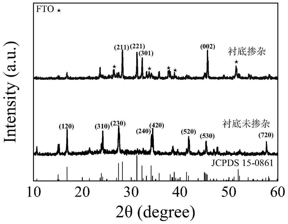
[0033] (3) In SnO 2 The electron transport layer was spin-coated at 2500 rpm for 60 s, and 20 mg / ml of CdCl was spin-coated 2 Doping treatment with methanol solution, and then annealing at 400°C for 60 min on a heating table to complete the doping treatment of the substrate film;

[0034] (4) The antimony selenide film was prepared by rapid thermal evaporation method, the vacuum ...


PUM


Abstract

The present invention is an induction (Sb 4 Se 6 ) n A method for preparing an antimony selenide photoelectric thin film with longitudinal growth of molecular chains, comprising a substrate thin film, which is characterized in that it also includes a dopant, and after the substrate thin film and the dopant prepare a doped substrate thin film, (Sb 4 Se 6 ) n Molecular chains can form covalent bonds with the substrate film, (Sb 4 Se 6 ) n The molecular chain grows along the vertical direction perpendicular to the substrate film, and finally induces a longitudinally preferred antimony selenide photoelectric thin film. Doping the substrate film can effectively improve the electrical properties of the product, so that the properties of the substrate film and the antimony selenide film are simultaneously improved, and finally the carrier transport performance of the antimony selenide optoelectronic device is effectively improved, and the optoelectronic performance is significantly improved. The method has the advantages of scientific and reasonable method, simple and practical preparation process, suitable for industrial production, low cost and high application value.

Description

technical field [0001] The invention belongs to the field of photoelectric thin film material and device preparation, and is an induced (Sb 4 Se 6 ) n A method for preparing an antimony selenide photoelectric thin film with longitudinal growth of molecular chains. Background technique [0002] Antimony selenide is a potential optoelectronic material. It not only has a narrow forbidden band width of 1 ~ 1.2eV, can effectively absorb the solar spectrum with a wavelength of less than 1100nm, but also has a high absorption coefficient, which is very suitable as a solar cell. and light absorbing layers of visible-near-infrared photodetectors. Antimony selenide is a one-dimensional chain structure in which one-dimensional (Sb 4 Se 6 ) n Molecular chains are held together by van der Waals forces, and the carriers along (Sb 4 Se 6 ) n The mobility of molecular chains is much greater than the transport rate between chains, so ensuring the vertical growth of antimony selenide...

Claims


Application Information

Patent Timeline
Patent Type & Authority Patents(China)
IPC IPC(8): C23C14/24C23C14/06C23C14/58C23C16/40H01L31/032H01L31/18
CPCC23C14/24C23C14/0623C23C14/5806C23C16/407H01L31/0321H01L31/186H01L31/1864Y02P70/50
Inventor 曹宇周静张鑫童孟丹唐喆庆蒋家豪刘超颖
Owner NORTHEAST DIANLI UNIVERSITY
Why Eureka
Try Eureka