Organic compound, electronic element and electronic device
A technology of organic compounds and chemical formulas, applied in organic chemistry, electrical components, organic semiconductor devices, etc., to achieve the effects of improving film formation and thermal stability, improving electron mobility, and improving luminous efficiency
- Summary
- Abstract
- Description
- Claims
- Application Information
AI Technical Summary
Problems solved by technology
Method used
Image

Examples
preparation example Construction
[0170] 1. Preparation of intermediates
[0171] (1) General synthesis process of intermediates sub 1 and sub 1'
[0172] Sub1 of the compound of the above chemical formula 1' and compound 2' can be synthesized by the following chemical reaction pathway, but is not limited thereto.
[0173]
[0174]
[0175] In the above ~ , Ar 1 、Ar 2 、X 1 、X 2 、X 3 and L 1 It has the meaning as in other parts of the description, Rs3 is selected from deuterium, halogen group, cyano group, alkyl group with 1 to 10 carbon atoms, haloalkyl group with 1 to 10 carbon atoms, and 6 to 10 carbon atoms. Aryl group with 20 carbon atoms, heteroaryl group with 3 to 20 carbon atoms, aryloxy group with 6 to 20 carbon atoms, arylthio group with 6 to 20 carbon atoms, silane with 3 to 12 carbon atoms A group consisting of an alkylamino group with 1 to 10 carbon atoms and a cycloalkyl group with 3 to 10 carbon atoms; L 2 ’, L 3 ’, L 4 , L 1 "is a substituted or unsubstituted arylene group with...
preparation example 1
[0176] (2) Preparation Example 1: The specific synthesis examples of the intermediate compounds Sub 1 and sub 1' are as follows.
[0177] Synthetic routes of Sub 1-B1 and Sub 1-C1
[0178]
[0179] 1) Synthesis of Sub 1-I-B1
[0180] 2-Chloro-4,6-diphenyl-1,3,5-triazine (20.00g, 74.70mmol), p-chlorophenylboronic acid (14.01g, 89.64mmol), tetrakistriphenylphosphine palladium (1.72g , 1.49mmol), potassium carbonate (22.71g, 164.35mmol), tetrabutylammonium chloride (4.15g, 14.94mmol), toluene (160mL), ethanol (80mL) and deionized water (40mL) into a three-necked flask, Under the protection of nitrogen, the temperature was raised to 78° C., heated to reflux and stirred for 8 hours. After the reaction, the solution was cooled to room temperature, added toluene (200mL) to extract the reaction solution, combined the organic phases, dried the organic layer over anhydrous magnesium sulfate, filtered, and concentrated; the crude product was purified by silica gel column chromatogra...
Embodiment 1
[0328] Embodiment 1: green organic electroluminescent device
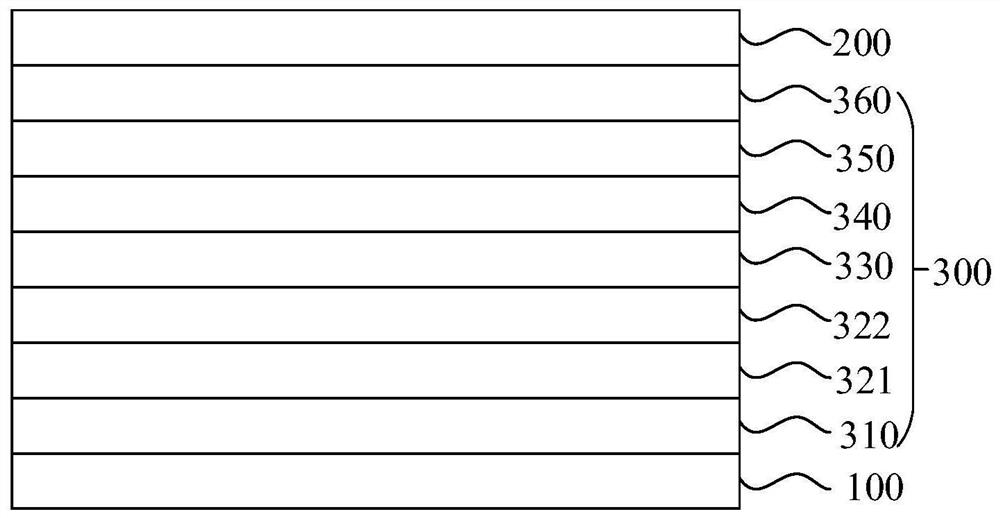
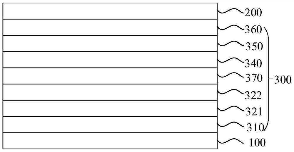
[0329] The anode was prepared by the following process: the ITO thickness was The substrate (manufactured by Corning) was cut into a size of 40mm × 40mm × 0.7mm, and it was prepared into an experimental substrate with cathode, anode and insulating layer patterns by using a photolithography process, using ultraviolet ozone and O 2 :N 2 Plasma surface treatment was performed to increase the work function of the anode (experimental substrate) and to remove scum.
[0330] HAT-CN was vacuum evaporated on the experimental substrate (anode) to form a thickness of The hole injection layer (HIL), and vacuum-evaporated NPB on the hole injection layer to form a thickness of hole transport layer (HTL).
[0331] Evaporate TCTA on the hole transport layer to form a thickness of electron blocking layer (EBL).
[0332] Using α,β-ADN as the host and doping BD-1 at the same time, the host and the dopant form a film with a ...
PUM
 Abstract
Description
Claims
Application Information
 - R&D
- Intellectual Property
- Life Sciences
- Materials
- Tech Scout
- Unparalleled Data Quality
- Higher Quality Content
- 60% Fewer Hallucinations
Browse by: Latest US Patents, China's latest patents, Technical Efficacy Thesaurus, Application Domain, Technology Topic, Popular Technical Reports.
© 2025 PatSnap. All rights reserved.Legal|Privacy policy|Modern Slavery Act Transparency Statement|Sitemap|About US| Contact US: help@patsnap.com