Transmission electron microscope high-resolution in-situ liquid phase temperature change chip and production method thereof
An in-situ liquid phase and transmission electron microscopy technology, which is applied in the preparation of test samples, material analysis using radiation, material analysis using wave/particle radiation, etc., can solve the limitations, single state of matter, and inability to achieve alternate transformation And other issues
- Summary
- Abstract
- Description
- Claims
- Application Information
AI Technical Summary
Problems solved by technology
Method used
Image

Examples
preparation example Construction
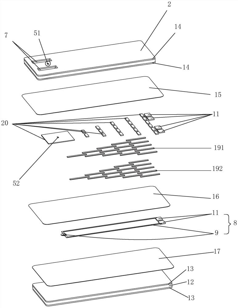
[0145] The preparation method of the upper sheet is as follows:
[0146] S1. Using the photolithography process, the central window pattern is transferred from the photolithography mask to the Si (100) wafer A with silicon nitride or silicon oxide layers on both sides, and then developed in the positive resist developing solution to obtain the wafer A-1;
[0147] Preferably, the photolithography process is exposed in the hard contact mode of the ultraviolet lithography machine; the thickness of the silicon nitride or silicon oxide layer is 5-200nm; the development time is 50s;
[0148] More preferably, the exposure time is 15s;
[0149] S2. Utilize the reactive ion etching process to etch a central window on the silicon nitride layer on the front side of the wafer A-1, then put the front side of the wafer A-1 up into acetone to soak, and finally use a large amount of Rinse with deionized water, remove the photoresist, and obtain wafer A-2;
[0150] S3. Using the ultraviolet...
Embodiment 1
[0201] Example 1: Preparation of a high-resolution in-situ liquid-phase temperature-changing chip by transmission electron microscopy
[0202] The preparation method of the upper sheet is,
[0203] S1. Using the photolithography process (exposure for 15s in the hard contact mode of the UV lithography machine), transfer the central window pattern from the photolithography mask to the Si(100) crystal with silicon nitride or silicon oxide layers on both sides. Circle A is then developed in positive photoresist developer for 50s to obtain wafer A-1; the thickness of the silicon nitride or silicon oxide layer is 5-200nm;
[0204] S2. Utilize the reactive ion etching process to etch a central window on the silicon nitride layer on the front side of the wafer A-1, then put the front side of the wafer A-1 up into acetone to soak, and finally use a large amount of Rinse with deionized water, remove the photoresist, and obtain wafer A-2;
[0205] S3. Using the ultraviolet laser direct...
Embodiment 2
[0231] Example 2: Use of a high-resolution in-situ liquid-phase temperature-changing chip for transmission electron microscopy
[0232] Inject an aqueous solution of supersaturated calcium hydroxide (the solution contains a small amount of calcium hydroxide particles) into the sample injection port of the transmission electron microscope high-resolution in-situ liquid phase temperature change chip prepared in Example 1. Temperature software, set the chip temperature to -30°C, get Figure 7 Electron microscope image from Figure 7 It can be seen from A and B that as the temperature rises, the solution temperature rises, the solubility of the solute gradually decreases, and calcium hydroxide solids are precipitated, and the nanoparticles are calcium hydroxide solids that are precipitated during the temperature rise of the chip. By controlling the amount of energization of the chip, the temperature of the solution in the chip can be monitored and controlled in real time. This t...
PUM
| Property | Measurement | Unit |
|---|---|---|
| Dimensions | aaaaa | aaaaa |
| Dimensions | aaaaa | aaaaa |
| Thickness | aaaaa | aaaaa |
Abstract
Description
Claims
Application Information