A micron-scale single crystal copper interconnect structure and preparation method thereof

An interconnection structure, single crystal copper technology, applied in semiconductor/solid-state device manufacturing, semiconductor/solid-state device components, semiconductor devices, etc. Improve the electroplating process and other problems to achieve the effects of excellent electrical conductivity, guaranteed transmission performance, and elimination of contributions

Active Publication Date: 2022-08-05
SHANGHAI JIAO TONG UNIV
View PDF4 Cites 0 Cited by
  • Summary
  • Abstract
  • Description
  • Claims
  • Application Information

AI Technical Summary

Problems solved by technology

[0005] In the existing research, there are attempts to increase the grain size, thereby reducing the number of grain boundaries to improve electrical conductivity, basically using the method of thermal annealing after electroplating, which can reduce the resistivity by about 8%, but these studies have not The influence of grain boundaries on electrical conductivity cannot be completely eliminated, and the electroplating process has not been improved. The help of additives is still needed, but the step of thermal annealing after electroplating is increased.
There are also researches that use electroless plating or electroplating to directly obtain nano-single crystal copper cones, but the electroless plating method has low repeatability and is not compatible with the preparation process of copper interconnection structures. The key to obtaining single crystal copper cones by electroplating is additives, and nanoscale is not suitable for copper interconnect structures

Method used


Image

  • A micron-scale single crystal copper interconnect structure and preparation method thereof
  • A micron-scale single crystal copper interconnect structure and preparation method thereof
  • A micron-scale single crystal copper interconnect structure and preparation method thereof

Examples


Embodiment 1

[0044] The preparation of the copper interconnect structure is simplified, and the most critical technology is to grow micron-scale single crystal copper needles from the phosphorous-containing copper seed layer. Other technologies are Damascus process, TSV process, and copper pillar bump process. normal operation. Therefore, the specific preparation operations are as follows:

[0045] (1) Use phosphorus-containing copper sheet instead of phosphorus-containing copper seed layer as the electroplating base. The phosphorous-containing copper sheet used is a commercial copper sheet produced by Kobelco Corporation of Japan, and contains 0.03 wt % of phosphorous.

[0046] (2) In the degreasing solution, the phosphorous copper sheet was cathode degreasing at a current density of 3ASD for 20 seconds, and rinsed with deionized water. The formula of degreasing liquid is 40g / L sodium hydroxide, 20g / L sodium carbonate, 1g / L sodium lauryl sulfate.

[0047] (3) The phosphor-containing co...

Embodiment 2

[0053] The difference between this embodiment and Embodiment 1 is that the sweep speed and interval are different, and the others are the same.

[0054] The specific differences are as follows: the scanning speed used in this embodiment is 1mV / s, and the scanning interval is 0.2-0.4V.

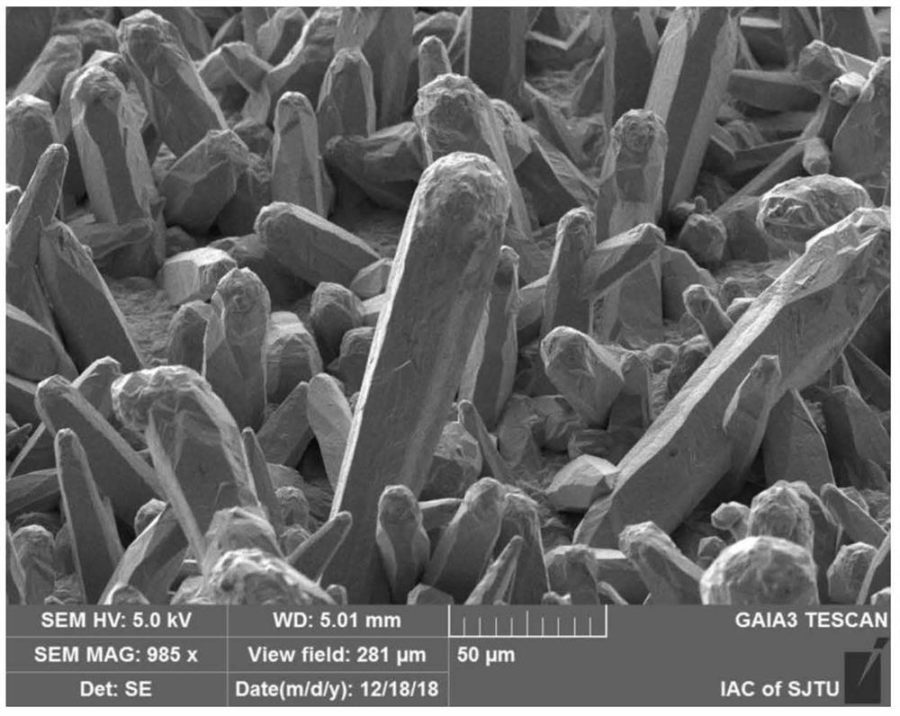
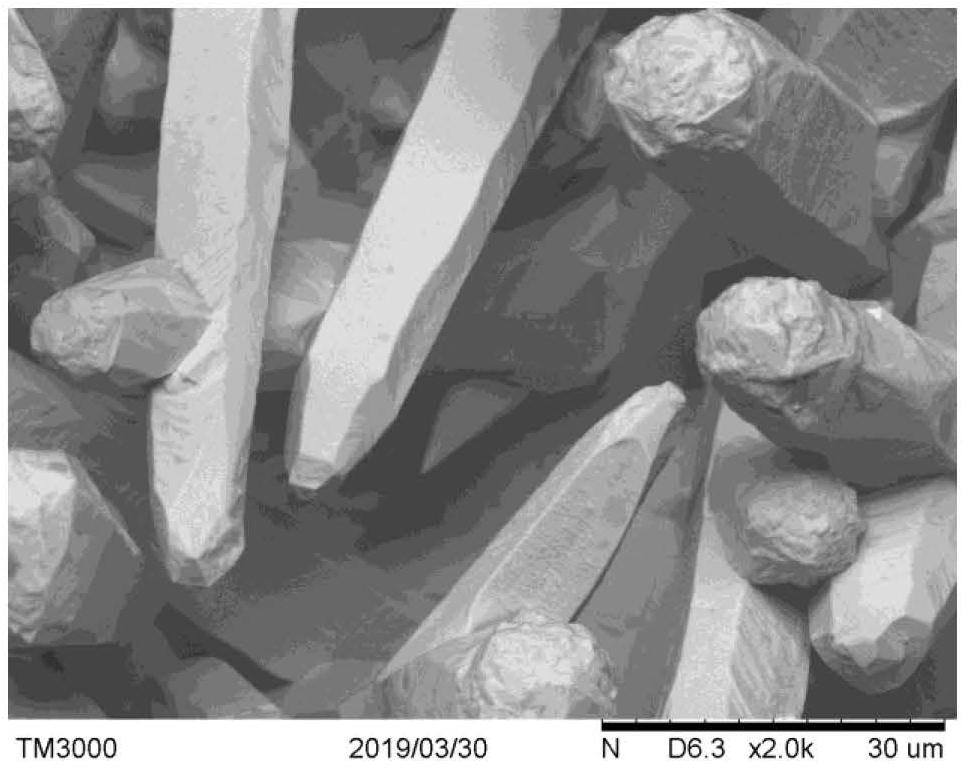
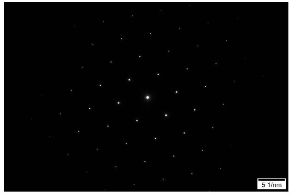
[0055] The resulting copper needles were longitudinally sectioned with FIB and imaged under FIB, as in Figure 4 shown. It can be seen that the width of the copper needle is 2-6 μm and the length is 5-25 μm. The color of the cross-section of a single copper needle is uniform and consistent, not as messy as the copper layer at the bottom, which can also indicate that the copper needle is a complete single crystal structure.

Embodiment 3

[0057] The present embodiment provides a method for preparing a micron-scale single-crystal copper interconnect structure using Damascus technology, including the following steps:

[0058] (1) Deposit a dielectric layer, the dielectric layer is a four-layer structure of silicon nitride-silicon oxide-silicon nitride-silicon oxide, located on the lower copper layer; A barrier layer is deposited by chemical vapor deposition on the inner sidewalls and bottoms of the through holes and trenches of the layer;

[0059] (2) The phosphorus-containing copper seed layer is deposited by the vacuum evaporation method with good deposition direction above the barrier layer parallel to the dielectric layer; the phosphorus content is about 0.03wt%;

[0060] (3) Pickling the phosphorous copper seed layer with dilute sulfuric acid with a volume fraction of 20% for 10s, and then applying a reverse current of 0.05A for 2000s to slightly dissolve the surface of the seed layer to ensure that the phos...


PUM

PropertyMeasurementUnit
widthaaaaaaaaaa
lengthaaaaaaaaaa
widthaaaaaaaaaa

Abstract

The invention discloses a micron-level single crystal copper interconnection structure and a preparation method thereof, belonging to the field of electronic packaging. The structure mainly includes a substrate, a barrier layer, a phosphorus-containing copper seed layer, and a copper needle; the substrate is a dielectric layer with through holes and grooves, a silicon wafer with blind holes, and a semiconductor substrate with copper pillar windows. A kind of; the barrier layer is arranged on the inner sidewall and bottom of the through hole and the trench of the dielectric layer, the inner sidewall and bottom of the blind hole of the silicon wafer, or the bottom of the copper column window on the semiconductor substrate; A phosphorous copper seed layer is disposed over the barrier layer parallel to the substrate; the copper needles are deposited on the phosphorous copper seed layer. In the structure, phosphorus element is doped into the copper seed layer, and the micron-scale single crystal copper needle can be formed as a copper interconnection structure without the assistance of additives during electroplating. The copper interconnection structure obtained by the invention is a complete single crystal structure, and there is no lateral grain boundary, so that the transmission performance of the copper interconnection is significantly improved.

Description

technical field [0001] The invention relates to the technical field of copper interconnection in electronic packaging, in particular to a micron-scale single crystal copper interconnection structure and a preparation method thereof. A micron-scale single crystal copper interconnect structure is prepared on the seed layer. The method can be applied to Damascus technology, TSV (through silicon via) technology, copper pillar bump technology, etc. in three-dimensional system-in-package. Background technique [0002] In deep submicron integrated circuits, three-dimensional system-in-package can effectively utilize the three-dimensional space, improve the packaging density, reduce the package volume, shorten the lead length, and improve the transmission speed. Among them, Damascus technology for interconnection between chips, TSV technology for interconnection between silicon wafers, copper pillar bump technology for interconnection between chips and substrates, etc., have become...

Claims


Application Information

Patent Timeline
Patent Type & Authority Patents(China)
IPC IPC(8): H01L23/48H01L23/528H01L23/532H01L21/768
CPCH01L23/481H01L23/5283H01L23/53228H01L23/53238H01L21/76877H01L21/7684H01L2224/11
Inventor 张若浔李明王淑慧谭祾月
Owner SHANGHAI JIAO TONG UNIV
Why Eureka
Try Eureka