A deep ultraviolet semiconductor light-emitting diode epitaxial structure
A technology of light-emitting diodes and epitaxial structures, which is applied to semiconductor devices, electrical components, circuits, etc., can solve the problems of reducing the internal quantum efficiency of deep ultraviolet LEDs, and cannot effectively improve the light extraction efficiency of deep ultraviolet LEDs, so as to improve light extraction efficiency, Improvement of light extraction efficiency and reduction of defect density
- Summary
- Abstract
- Description
- Claims
- Application Information
AI Technical Summary
Problems solved by technology
Method used
Image
Examples
Embodiment 1
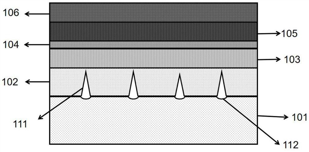
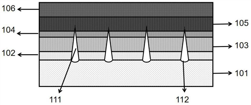
[0048] The epitaxial structure of the DUV LED of this embodiment, such as figure 2 As shown, along the epitaxial direction, it includes a pattern substrate 101, a semiconductor buffer layer 102, an n-type semiconductor material layer 103, an n-type semiconductor material layer 103, a multiple quantum well layer 104, a p-type electron blocking layer 105, and a p-type semiconductor material layer. transport layer 106;
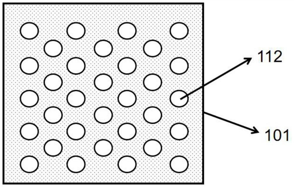
[0049] The graphics substrate, such as image 3 As shown, regularly arranged grooves 112 are etched on the graphics substrate 101. The grooves 112 are pits with a diameter between 500nm and 550nm and a depth between 250nm and 300nm. The grooves 112 are on the graphics substrate 101. Graphic arrangement, the present embodiment is a rectangular square matrix arrangement (such as image 3 shown), with a pitch of 20 μm.
[0050] Wherein, a cavity structure is grown on each groove 112 on the surface of the graphics substrate 101, the cavity structure passes throug...
Embodiment 2
[0065] Other steps are the same as in Embodiment 1, except that the size of the substrate pattern etched on the substrate by nanoimprinting or holographic lithography technology is larger, with a diameter between 2-4 μm and a depth between 1-2 μm. This results in a cavity that completely penetrates the entire epitaxial structure, such as Figure 6 As shown, that is, the cavity is in an unclosed state when the growth of the epitaxial structure is completed.
[0066]In addition, the arrangement of the substrate graphics can also be in a circular radial arrangement with an arrangement spacing of 2-200 μm; the substrate graphics can be rectangular strips or other irregular geometric figures with an area of 0.25-400 μm 2 In addition to sapphire, the substrate can also be aluminum nitride, gallium nitride, 4H-SiC, R-surface aluminum oxide single crystal, gallium oxide, 6H-SiC, etc.
PUM
| Property | Measurement | Unit |
|---|---|---|
| size | aaaaa | aaaaa |
| size | aaaaa | aaaaa |
| depth | aaaaa | aaaaa |
Abstract
Description
Claims
Application Information


