Vertical Ga2O3 nanotube ordered array and preparation method thereof
A technology of ordered arrays and nanotubes, applied in nanostructure manufacturing, nanotechnology, nanotechnology, etc., can solve difficult problems such as direction, length, size and tube wall thickness
- Summary
- Abstract
- Description
- Claims
- Application Information
AI Technical Summary
Problems solved by technology
Method used
Image

Examples
Embodiment 1
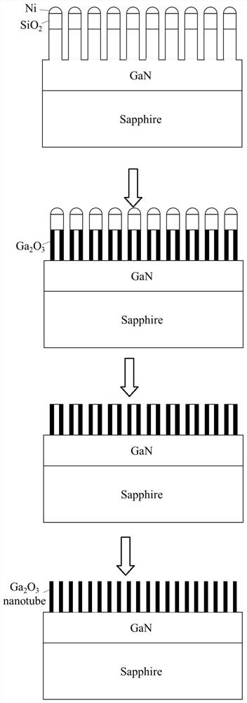
[0037] a vertical Ga 2 o 3 A method for preparing an ordered array of nanotubes, the steps comprising:
[0038] (1) The device is ultrasonically cleaned with acetone, ethanol, and deionized water in sequence, and then dried with nitrogen, wherein the device is a GaN film grown on the substrate;
[0039] (2) Using plasma-enhanced chemical vapor deposition to grow a layer of SiO with a thickness of 200 nm on the cleaned device 2 Thin film, and then a layer of Ni metal film with a thickness of 20nm is deposited by electron beam evaporation;
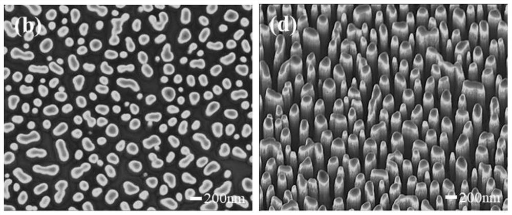
[0040] (3) annealing the above metal-plated device to form a Ni metal nanoparticle structure used as an etching mask on the surface, the annealing temperature is 850 ° C, and the time is 10 min;
[0041] (4) Put the annealed device into RIE and ICP etching equipment sequentially, and use Ni metal nanoparticles as a mask to perform a dry etching process, wherein the RIE etching conditions: the etching gas is CF 4 / O 2 , the flow ratio is...
Embodiment 2
[0046] a vertical Ga 2 o 3 A method for preparing an ordered array of nanotubes, the steps comprising:
[0047] (1) The device is ultrasonically cleaned with acetone, ethanol, and deionized water in sequence, and then dried with nitrogen, wherein the device is a GaN film grown on the substrate;
[0048] (2) on the device after cleaning, be the Ni metal thin film of 5nm by electron beam evaporation coating one deck thickness;
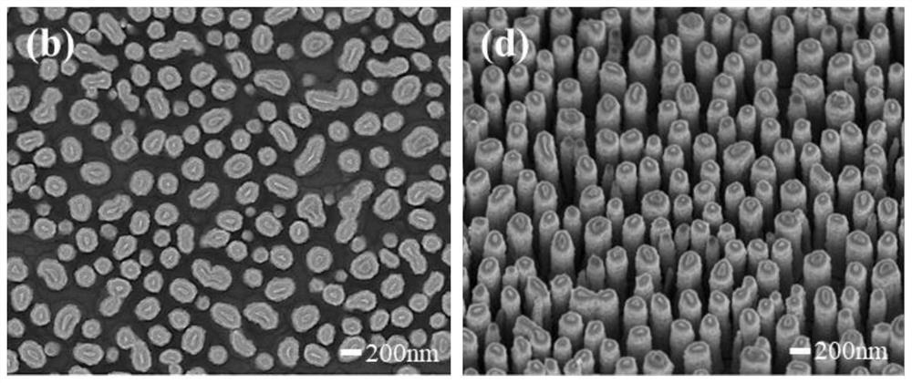
[0049] (3) annealing the above metal-coated device to form a Ni metal nanoparticle structure used as an etching mask on the surface, the annealing temperature is 750 ° C, and the time is 1 min;
[0050] (4) Put the annealed device into the ICP etching equipment and use Ni metal nanoparticles as a mask to perform a dry etching process. ICP etching conditions: the etching gas is Cl 2 / BCl 3 , the flow ratio is 24 / 6sccm, the etching power is 50 / 100W, the chamber pressure is 5mTorr, and the etching time is 4min to obtain an ordered array of vertical GaN ...
Embodiment 3
[0055] a vertical Ga 2 o 3 A method for preparing an ordered array of nanotubes, the steps comprising:
[0056] (1) The device is ultrasonically cleaned with acetone, ethanol, and deionized water in sequence, and then dried with nitrogen, wherein the device is a GaN film grown on the substrate;
[0057] (2) Using plasma-enhanced chemical vapor deposition to grow a layer of SiO with a thickness of 400 nm on the cleaned device 2 Thin film, and then a layer of Ni metal film with a thickness of 50nm is deposited by electron beam evaporation;
[0058] (3) annealing the above metal-plated device to form a Ni metal nanoparticle structure used as an etching mask on the surface, the annealing temperature is 950 ° C, and the time is 20 min;
[0059] (4) Put the annealed device into RIE and ICP etching equipment sequentially, and use Ni metal nanoparticles as a mask to perform a dry etching process, wherein the RIE etching conditions: the etching gas is CF 4 / O 2 , the flow ratio is...
PUM
| Property | Measurement | Unit |
|---|---|---|
| thickness | aaaaa | aaaaa |
| thickness | aaaaa | aaaaa |
| strength | aaaaa | aaaaa |
Abstract
Description
Claims
Application Information
 - R&D
- Intellectual Property
- Life Sciences
- Materials
- Tech Scout
- Unparalleled Data Quality
- Higher Quality Content
- 60% Fewer Hallucinations
Browse by: Latest US Patents, China's latest patents, Technical Efficacy Thesaurus, Application Domain, Technology Topic, Popular Technical Reports.
© 2025 PatSnap. All rights reserved.Legal|Privacy policy|Modern Slavery Act Transparency Statement|Sitemap|About US| Contact US: help@patsnap.com