Monocrystalline silicon wafer with grooves in surface, heterojunction solar cell and preparation method

A technology of monocrystalline silicon wafers and solar cells, applied in circuits, electrical components, photovoltaic power generation, etc., can solve problems such as large series resistance, high light shading, and large silver paste consumption, so as to increase speed, reduce shading area, The effect of reducing the requirements of bonding ability and setting ability

Active Publication Date: 2021-08-31
SHANGHAI INST OF MICROSYSTEM & INFORMATION TECH CHINESE ACAD OF SCI
View PDF7 Cites 2 Cited by
  • Summary
  • Abstract
  • Description
  • Claims
  • Application Information

AI Technical Summary

Problems solved by technology

[0005] In view of the shortcomings of the prior art described above, the purpose of the present invention is to provide a single crystal silicon wafer with grooves on the surface, a heterojunction solar cell and a preparation method, which are used to solve the problem of heterojunction solar cells in the prior art. There are many deficiencies in the preparation of electrodes using low-temperature silver paste, including high light shading caused by the low aspect ratio of the grid lines, large series resistance caused by poor contact between the grid lines and the TCO film, and the adhesion between the grid lines and the TCO film. Low welding tension caused by weakness, high battery cost caused by large consumption of silver paste, etc.

Method used


Image

  • Monocrystalline silicon wafer with grooves in surface, heterojunction solar cell and preparation method
  • Monocrystalline silicon wafer with grooves in surface, heterojunction solar cell and preparation method
  • Monocrystalline silicon wafer with grooves in surface, heterojunction solar cell and preparation method

Examples


preparation example Construction

[0055] The present invention also provides a method of preparing a single crystal silicon wafer having a groove as described in any of the above, comprising the steps of:

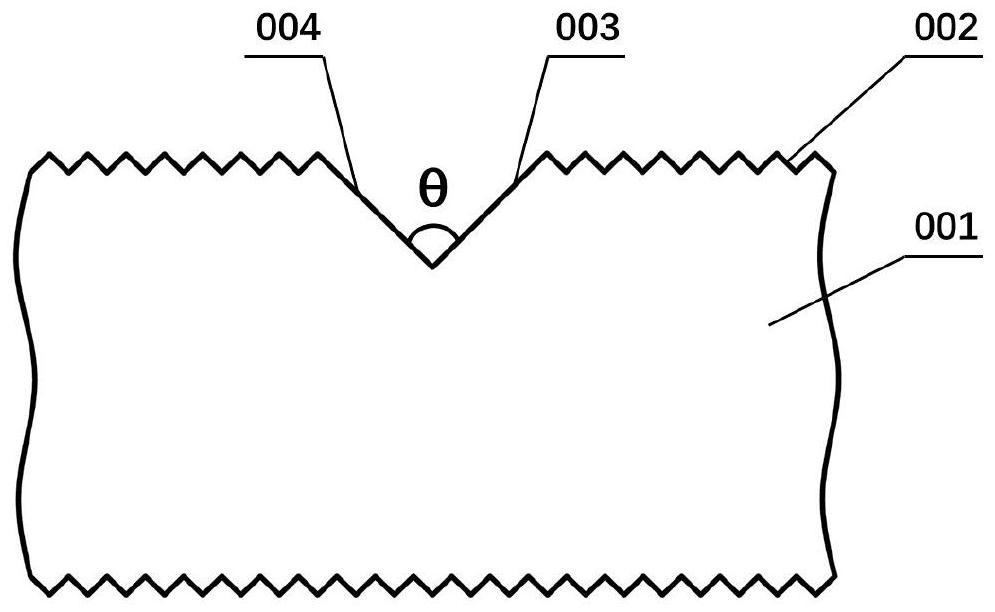
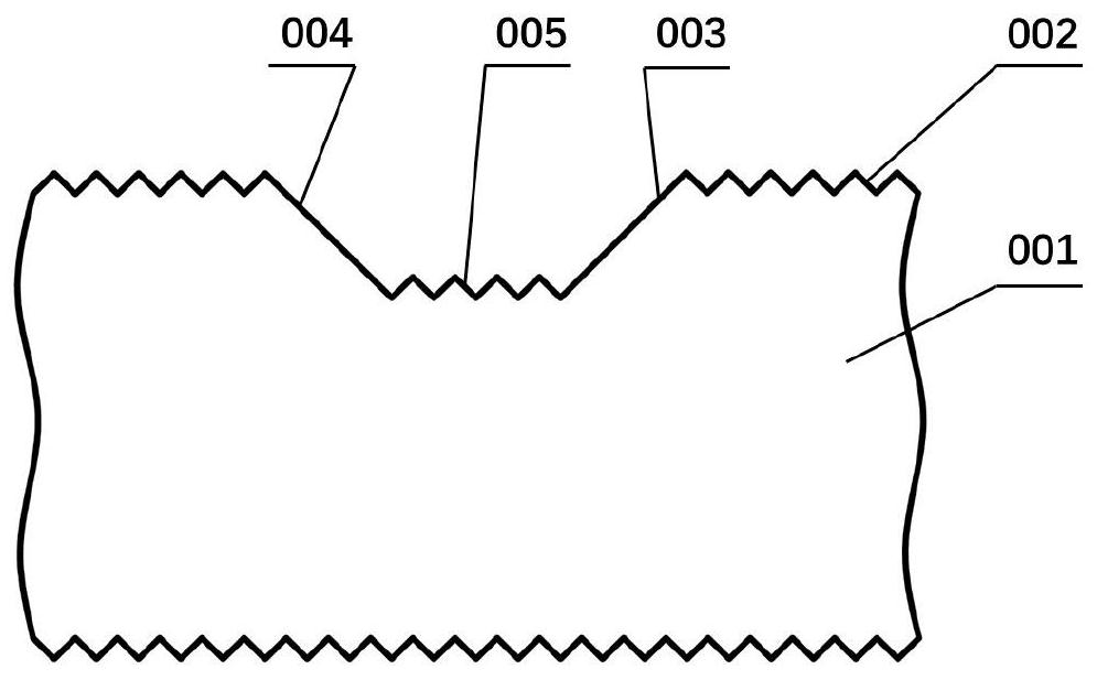
[0056] S1: According to the preset graphics, the laser etching process is applied to the front side of the single crystal silicon wafer and the back surface, respectively, such as the graphics of the front gate line of the solar cell and the back gate line. The front and back surface of the crystalline silicon wafer erates a groove having a certain depth and width, depending on the width of the groove, the number of grooves and the number of gate lines may or inconsistent, such as if the groove width is narrow, one The gate line can correspond to a groove of two and more, and the number of grooves is larger than the number of gate lines;

[0057] S2: Corrosion wafer in the alkaline solution, so that the groove width of the laser-etched, the inner surface and the surface of the groove becomes more flat, the alka...

Embodiment 1

[0070] This example is used to prepare a single crystal silicon wafer having a groove provided by the first surface provided by the present invention (eg figure 1 ),Specific steps are as follows:

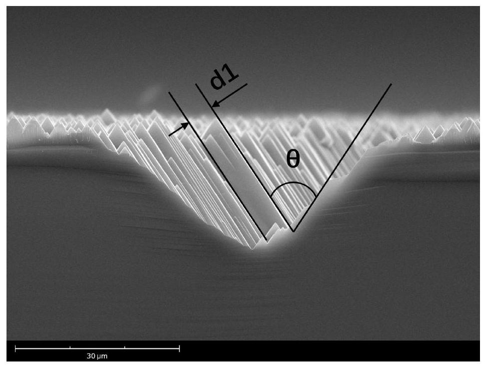
[0071] (1) Laser split groove: According to the battery grid line pattern, the front and back surface of the single crystal silicon wafer, respectively, the groove depth is 16 μm, the groove width is 15 μm, and the front gate line pattern is like Figure 13 As shown, the back gate line pattern is like Figure 14 Indicated;

[0072] (2) Ozone cleaning: Wash the silicon sheet in the mixed solution of ozone and hydrofluoric acid, the ozone concentration is 30 ppm, the mass fraction of hydrofluoric acid is 1%, the temperature is 25 ° C, the time is 3 min, then rinsing in pure water Silicon film 2min;

[0073] (3) Alkali polishing: Corrosion wafer in KOH solution, the mass fraction of KOH is 7%, the temperature is 80 ° C, then the time is 3 min, then rinsing the silicon wafer in pure water 2mi...

Embodiment 2

[0090] This example is used to prepare a single crystal silicon wafer having a groove provided by the second surface provided by the present invention, and the specific steps are as follows:

[0091] (1) Laser splitting: according to the battery grid line pattern, the laser etching groove is applied to the back surface, respectively, the groove depth is 16 μm, the groove width is 15 μm; the front gate line pattern is like Figure 13 , Back gate line graphic Figure 14 Indicated;

[0092] (2) Ozone cleaning: Wash the silicon sheet in the mixed solution of ozone and hydrofluoric acid, the ozone concentration is 30 ppm, the mass fraction of hydrofluoric acid is 1%, the temperature is 25 ° C, the time is 3 min, then rinsing in pure water Silicon film 2min;

[0093] (3) Alkali polishing: Corrosion silicon wafers in KOH solution, the mass fraction of KOH is 7%, the temperature is 80 ° C, the time is 6 min, then the wafer is rinsed in pure water 2min; the alkali polished recess Section of ...


PUM

PropertyMeasurementUnit
depthaaaaaaaaaa
widthaaaaaaaaaa
heightaaaaaaaaaa

Abstract

The invention provides a monocrystalline silicon wafer with grooves in the surface, a heterojunction solar cell and a preparation method. Grooves are formed in the front face and the back face of the silicon wafer, the depth of each groove ranges from 5 micrometers to 50 micrometers, the width of each groove ranges from 10 micrometers to 100 micrometers, the internal morphology of each groove comprises one or two of a step shape and a pyramid shape, the surface morphology of the monocrystalline silicon wafer outside the grooves comprises a pyramid shape, and the surfaces of the steps and the pyramid correspond to the crystal face (111) of the silicon crystal. The distance between adjacent step edges on the same inclined plane is 0.1-10 [mu]m, and the height of the pyramid is 0.1-10 [mu]m. When the method is used for preparing the heterojunction solar cell, the contact area of the grid line and the transparent conductive film can be increased, the filling factor FF of the solar cell and the welding tension of the electrode can be improved, the shading area of the grid line can be reduced, and the short-circuit current Isc can be obviously improved; meanwhile, consumption of silver paste can be reduced, and efficiency improvement and cost reduction of the solar cell are achieved. In addition, the conductive performance of the silver paste and the speed of silk-screen printing are improved, so that the productivity of equipment is improved.

Description

Technical field [0001] The present invention relates to a silicon wafer and the texturing art heterojunction solar cells, particularly relates to a surface-single-crystal silicon substrate having a recess, and a preparation method of heterojunction solar cells. Background technique [0002] Heterojunction solar cells the conversion efficiency of the solar cell is generally higher than PERC, it has a simple structure, high open-circuit voltage, temperature characteristics, power generation, etc. can be two-sided. Heterojunction cell made using a low temperature process, the maximum temperature is generally no more than 250 deg.] C, higher temperatures can cause the amorphous silicon thin film silicon hydrogen bonds, the passivation performance deteriorates, reducing the conversion efficiency of the battery, so heterojunction cell preparing an electrode using a low temperature process is also required, usually by way of screen printing, the conductive silver paste printed on the fr...

Claims


Application Information

Patent Timeline
Patent Type & Authority Applications(China)
IPC IPC(8): H01L31/0747H01L31/0352H01L31/0236H01L31/036H01L31/0224H01L31/20
CPCH01L31/0747H01L31/035281H01L31/02363H01L31/036H01L31/022433H01L31/202Y02P70/50Y02E10/50
Inventor 杜俊霖韩安军刘正新孟凡英张丽平石建华
Owner SHANGHAI INST OF MICROSYSTEM & INFORMATION TECH CHINESE ACAD OF SCI
Why Eureka
Try Eureka