A circular waveguide based on thin film self-curling technology

A self-curling and circular waveguide technology, applied in the field of on-chip terahertz wave transmission and circular waveguide, can solve problems such as the difficulty of terahertz wave transmission, and achieve the effects of high conductivity, superior structural performance, and high charge transmission efficiency

Active Publication Date: 2022-03-18
KUNSHAN RUIXIANG XUNTONG COMM TECHCO
View PDF7 Cites 0 Cited by
  • Summary
  • Abstract
  • Description
  • Claims
  • Application Information

AI Technical Summary

Problems solved by technology

Terahertz is a new radiation source with many unique advantages; Terahertz technology is a very important cross-frontier field, which provides a very attractive opportunity for technological innovation, national economic development and national security, but the realization of too Transmission of Hertzian waves is difficult

Method used


Image

  • A circular waveguide based on thin film self-curling technology
  • A circular waveguide based on thin film self-curling technology
  • A circular waveguide based on thin film self-curling technology

Examples


Embodiment 1

[0050] A kind of circular waveguide preparation operation steps based on film self-curling technology is as follows:

[0051] (1) slice and wash

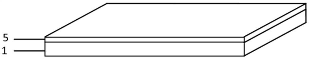
[0052] Take a complete silicon wafer and use a diamond pen to cut it into a rectangular silicon wafer with an area of ​​0.6cm×0.3cm as the silicon substrate 1 . Wash with methanol solution followed by isopropanol (IPA) solution, then blow dry with nitrogen gun.

[0053] (2) Deposit germanium metal layer

[0054] Using vacuum coating machine equipment, the vacuum degree during coating is high vacuum degree 10 -3 -10 -4 Pa. Electron beam evaporation technology is used to deposit germanium metal layer 5 on silicon substrate 1, the thickness of germanium metal layer 5 is 70nm, see figure 2 .

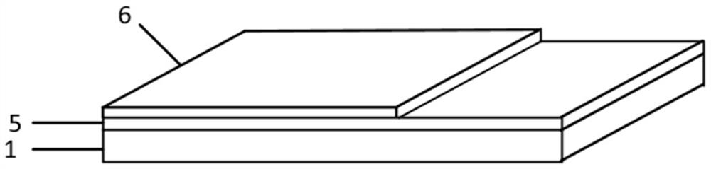
[0055] (3) Coating positive photoresist, exposure, development

[0056]The silicon substrate sheet 1 is film-formed using hexamethylsilazane (HMDS), which functions as an adhesion promoter. Immediately apply a liquid-phase positive photor...

Embodiment 2

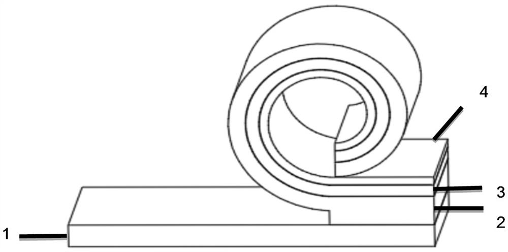
[0073] Such as figure 1 For the circular waveguide shown, the inner diameter of the circular waveguide in Embodiment 2 is 48um, and the specific process flow is the same as in Embodiment 1.


PUM

PropertyMeasurementUnit
thicknessaaaaaaaaaa
thicknessaaaaaaaaaa
thicknessaaaaaaaaaa

Abstract

The invention relates to a circular waveguide based on the film self-curling technology, which belongs to the technical field of nanometer devices. Using a silicon wafer as a substrate, a titanium metal layer, a copper metal layer and a gold metal layer are deposited on the substrate, and by etching the germanium sacrificial layer, the internal stress between different metal layers is used to trigger the titanium, copper, and gold metal layers to automatically curling, thereby realizing the transition from two-dimensional to three-dimensional, forming self-curling micro-nanotubes. The inner diameter of the micro-nanotube is in the order of microns, and the working frequency of the circular waveguide is in the terahertz band. The on-chip circular waveguide structure made by the present invention is miniaturized, and the micro-nanotube structure of the nano-film provides superior structural performance, high electrical conductivity and charge transmission efficiency; the manufacturing method of the present invention is easy to operate and lower in cost , can be mass produced.

Description

technical field [0001] The invention belongs to the technical field of nanometer devices, and relates to a circular waveguide formed based on self-curling film nanotechnology, which realizes the transmission of terahertz waves on a chip. Background technique [0002] Traditional waveguides can be divided into two types: ordinary waveguides and slotted waveguides. Ordinary waveguide is a hollow metal conduit with a very smooth inner wall or a metal-coated tube. The waveguide is used to transmit ultra-high frequency electromagnetic waves. The common cross-sectional shapes are rectangular and circular, and the cross-sectional shape is circular. It is a circular waveguide through which the pulse signal is transmitted to the destination with minimal loss. The size of the inner diameter of the waveguide varies with the wavelength of the transmitted signal. The traditional circular waveguide has a large volume, and the inner diameter is on the order of millimeters to centimeters, ...

Claims


Application Information

Patent Timeline
Patent Type & Authority Patents(China)
IPC IPC(8): H01P3/12H01P3/127H01P11/00B81B1/00B81C1/00
CPCH01P3/121H01P3/127H01P11/001B81B1/002B81C1/00023
Inventor 黄文汪颖宇景辉桑磊
Owner KUNSHAN RUIXIANG XUNTONG COMM TECHCO
Why Eureka
Try Eureka