Secondary epitaxy method of N-type heavily-doped thin-layer gallium nitride material

A secondary epitaxy and heavy doping technology, applied in the secondary epitaxy field of gallium nitride materials, can solve the problems of aggravating the deterioration of GaN crystal quality, increase in resistivity, and high requirements for vacuum conditions, and improve material quality and surface morphology. , reduce ohmic contact resistance, improve the effect of parasitic effects

Pending Publication Date: 2021-12-17
NO 55 INST CHINA ELECTRONIC SCI & TECHNOLOGYGROUP CO LTD
View PDF0 Cites 1 Cited by
  • Summary
  • Abstract
  • Description
  • Claims
  • Application Information

AI Technical Summary

Problems solved by technology

Silane is the most commonly used N-type doping source in GaN materials. However, the radius of silicon atoms and gallium atoms is quite different. Doping too high a dose of silicon atoms in the material will cause distortion of the GaN lattice, resulting in GaN crystal quality and surface There is a more obvious degradation of the morphology
MBE technology has excellent characteristics such as atomic-level orderly accretion, highly clean growth surface and atomic-level flatness, which is conducive to alleviating lattice distortion under heavy doping, and realizing N-type with higher crystal quality and smoother surface Heavily doped thin-layer materials, but there are disadvantages such as low growth rate, high requirements for vacuum conditions, and low yield, so it is not suitable for large-scale production
MOCVD and other technologies have the characteristics of fast growth and large production capacity, and are suitable for mass production. However, N-type GaN materials are limited by lattice distortion under heavy doping, and GaN is injected with high-concentration silane during MOCVD high-temperature epitaxial growth. Some silanes will react with NH 3 A chemical vapor phase reaction occurs to generate amorphous silicon nitride and embed it into the GaN lattice. While aggravating the degradation of GaN crystal quality, it reduces the efficiency of silicon atoms being incorporated into the GaN lattice, resulting in an increase in the resistivity of N-type heavily doped GaN materials. , is not conducive to reducing the ohmic contact resistance

Method used


Image

  • Secondary epitaxy method of N-type heavily-doped thin-layer gallium nitride material
  • Secondary epitaxy method of N-type heavily-doped thin-layer gallium nitride material
  • Secondary epitaxy method of N-type heavily-doped thin-layer gallium nitride material

Examples


Embodiment Construction

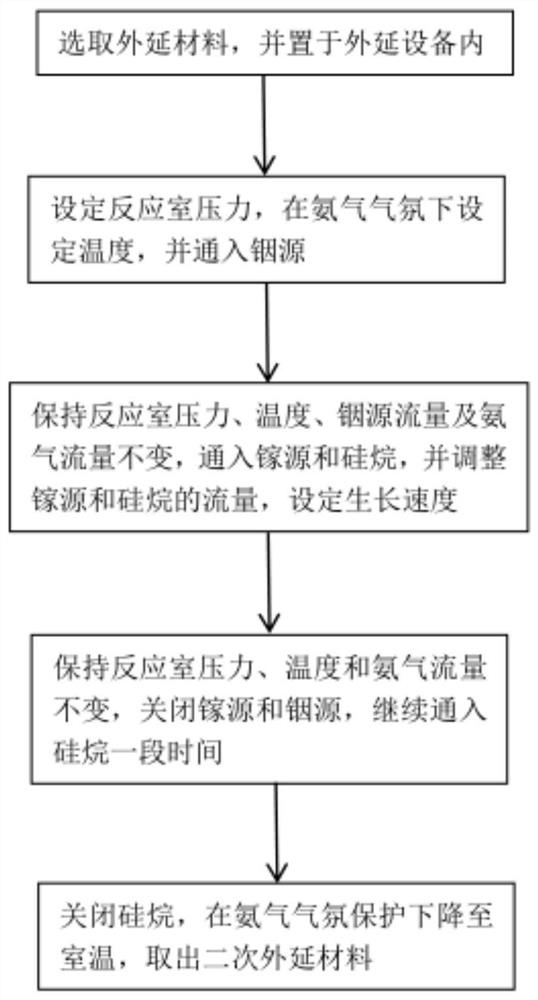
[0022] The present invention will be further described in detail below in conjunction with the accompanying drawings and specific embodiments.

[0023] The secondary epitaxy method of thin-layer GaN material of the present invention, as figure 1 The flowchart shown includes the following steps:

[0024] (1) Select the surface of III-V nitrides such as GaN as the epitaxial material, or the surface of various semiconductor materials and devices as the epitaxial material, and place it in MOCVD (Metal-organic Chemical Vapor Deposition) and other epitaxial growth on the base of the device.

[0025] (2) Set the pressure of the reaction chamber as P, and the ammonia gas (NH 3 ) atmosphere to raise the temperature of the reaction chamber to T, and then feed the flow rate of 1×10 -5 ~1×10 -4 mol / min indium source, and last for 0.5-2min (minutes).

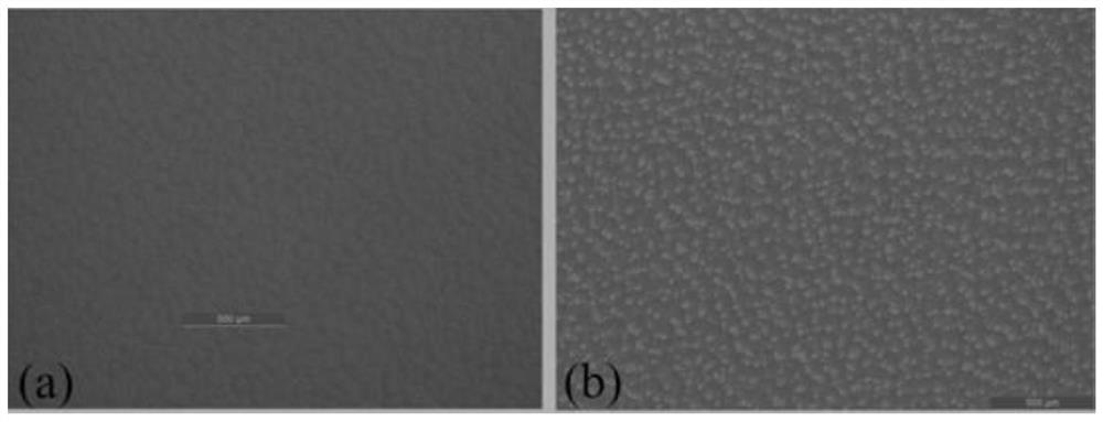
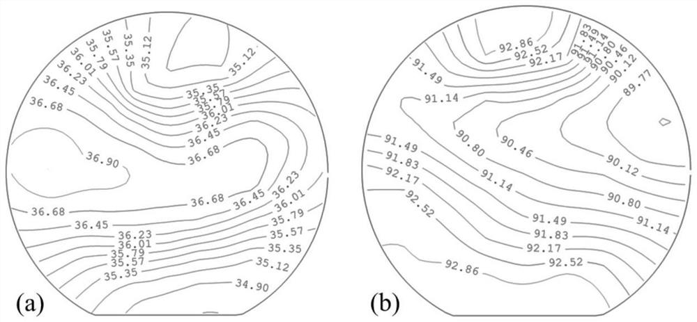
[0026] The growth temperature T ranges from 830 to 990°C. In order to suppress the N-type heavily doped GaN material during the secon...


PUM

PropertyMeasurementUnit
thicknessaaaaaaaaaa
temperatureaaaaaaaaaa
electrical resistivityaaaaaaaaaa

Abstract

The invention discloses a secondary epitaxy method of an N-type heavily-doped thin-layer gallium nitride material. The method comprises the following steps: (1) selecting an epitaxial material, and placing the epitaxial material on a base in MOCVD epitaxial growth equipment; (2) setting the pressure of a reaction chamber, heating the reaction chamber to a preset temperature in an ammonia gas atmosphere, and then continuously introducing an indium source; (3) keeping the pressure, the temperature, the indium source flow and the ammonia gas flow of the reaction chamber unchanged, and introducing a gallium source and silane; adjusting the flow of the gallium source and the indium source, setting the growth rate, and starting secondary epitaxy of the N-type heavily doped thin layer GaN material; (4) keeping the pressure, the temperature and the ammonia gas flow of the reaction chamber unchanged, closing the gallium source and the indium source, and continuously introducing silane for a period of time; and (5) closing the silane, cooling to room temperature under the protection of ammonia gas atmosphere, and taking out the secondary epitaxial material. The N-type heavily-doped thin-layer GaN material is good in surface appearance and high in crystallization quality, and ohmic contact resistance of a high-frequency GaN power device can be reduced.

Description

technical field [0001] The invention relates to a secondary epitaxy method for gallium nitride materials, in particular to a secondary epitaxy method for N-type heavily doped thin-layer gallium nitride materials. Background technique [0002] Gallium nitride (GaN) microwave power devices have the characteristics of large output power, high operating frequency, high temperature resistance, etc., and are widely used in wireless communication base stations, radio frequency energy and other fields. In order to further improve frequency performance and maintain high drive current and output power, GaN power devices in the W-band and above frequency bands have a higher aluminum composition in the barrier layer and a larger band gap on the surface of the material, which leads to the use of alloyed ohmic The contact resistance obtained by techniques such as contact and ohmic area etching is generally too large, resulting in obvious parasitic effects, which seriously limits the perfo...

Claims


Application Information

Patent Timeline
Patent Type & Authority Applications(China)
IPC IPC(8): H01L21/02C30B25/02C30B25/16C30B29/40
CPCH01L21/02458H01L21/0254H01L21/0262C30B25/02C30B29/406C30B25/16
Inventor 李传皓李忠辉彭大青
Owner NO 55 INST CHINA ELECTRONIC SCI & TECHNOLOGYGROUP CO LTD
Why Eureka
Try Eureka