Photomask blank, method for producing photomask, and photomask
A photomask and light-shielding film technology, applied in the field of photomasks, can solve the problems of insufficient etching and reduction, and achieve the effect of achieving resolution limit, high adhesion, and good resolution limit
- Summary
- Abstract
- Description
- Claims
- Application Information
AI Technical Summary
Problems solved by technology
Method used
Image
Examples
Embodiment 1
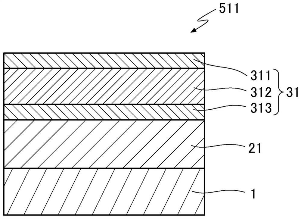
[0119] Manufactured a phase shift film (halftone phase shift film) which is a film made of a material containing silicon and a hard mask which is a film made of a material containing chromium on a transparent substrate made of quartz with a size of 152 mm square and a thickness of about 6 mm. Mold-film-laminated, photomask blanks (halftone phase-shift blanks).
[0120] First, on a transparent substrate, a molybdenum target and a silicon target are used as targets, the power applied to the targets is adjusted, and argon gas and nitrogen gas are used as sputtering gases, and sputtering is performed in these gas atmospheres to form a single-layer film. A MoSi-based phase shift film (thickness: 70 nm) made of MoSiN, having a phase difference of 177 degrees with respect to light having a wavelength of 193 nm, and a transmittance of 6% (optical density: 1.2) was prepared.
[0121] Next, on the phase shift film, a chromium target was used as a target, the power applied to the target ...
Embodiment 2
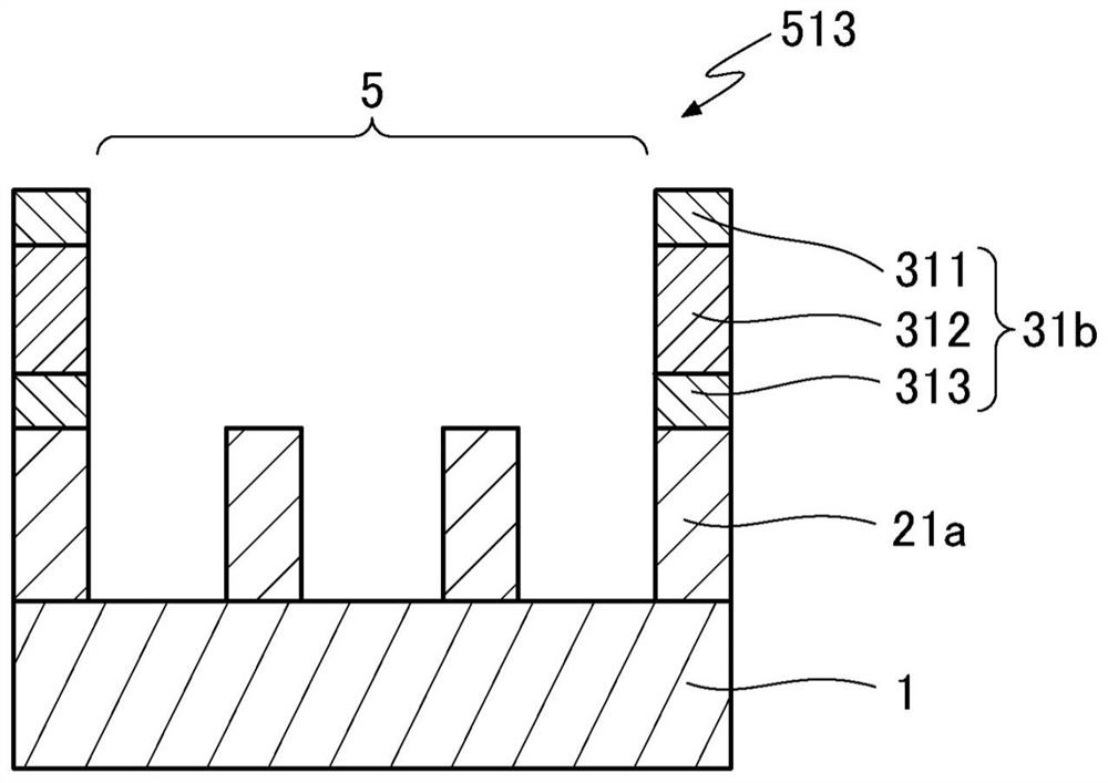
[0126] In order to evaluate the resolution limit of the fine pattern equivalent to the auxiliary pattern of the line pattern, using the photomask blank including the resist film obtained in Example 1, according to Figure 7 The process shown in produces figure 2 The photomask (halftone phase-shift mask) shown in .
[0127] First, a photomask blank including a resist film ( Figure 7 (A)). Secondly, using the electron beam drawing device, with a dose of 35 μC / cm 2 A test pattern corresponding to the auxiliary pattern of the line pattern was created, and a total of 200,000 isolated patterns with different short-side dimensions were drawn with a long-side size of 140 nm and a short-side size changed from 20 nm to 100 nm every 2 nm. Then, heat treatment was performed at 110° C. for 14 minutes using a heat treatment apparatus (PEB: Post Exposure Bake). Secondly, adopt immersion developing to carry out 100 second developing process, have formed resist pattern ( Figure 7 (B))....
Embodiment 3
[0144] In order to evaluate the influence accompanying the peeling of the resist film formed on the film made of a material containing chromium using the resolution limit of the fine pattern equivalent to the auxiliary pattern of the line pattern, the resist film obtained in Example 1 was used. agent film photomask blank, according to Figure 8 and Figure 7 The process shown in produces figure 2 The photomask (halftone phase-shift mask) shown in .
[0145] First, a photomask blank including a resist film ( Figure 8 (A)). Next, the resist film was peeled off by washing with sulfuric acid hydrogen peroxide water for 12 minutes. Then, in order to neutralize the sulfate ions remaining on the surface of the hard mask film (first layer), it was rinsed with ammonia-added water (ammonia hydrogen peroxide water, APM) for 15 minutes. (Layer 1) The surface was reduced by adding water to the ammonia, and carried out a 15-minute dry spin-coating rinse ( Figure 8(B)). Next, a neg...
PUM
| Property | Measurement | Unit |
|---|---|---|
| thickness | aaaaa | aaaaa |
| thickness | aaaaa | aaaaa |
| thickness | aaaaa | aaaaa |
Abstract
Description
Claims
Application Information


