Planar conjugated molecule compound and monomolecular field effect transistor comprising same
A technology of field-effect transistors and molecular compounds, applied in the field of single-molecule field-effect transistors, can solve problems such as poor stability and integration, sensitivity to dielectric layer thickness, and difficult process implementation, and achieve good conjugation, face-to-face stacking, The effect of strong grid electric field control ability
- Summary
- Abstract
- Description
- Claims
- Application Information
AI Technical Summary
Problems solved by technology
Method used
Image

Examples
preparation example Construction
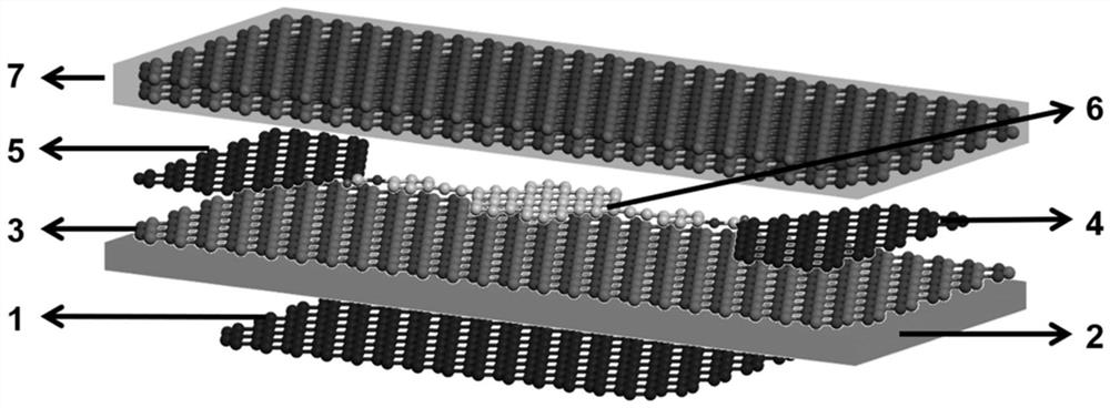
[0056] The third aspect of the present application provides the preparation method of the unimolecular field effect transistor provided in the second aspect of the present application, which includes the following steps:
[0057] 1) preparing a graphene gate electrode layer on the substrate;
[0058] 2) Preparation of Bi on the upper surface of the graphene gate electrode layer 2 SeO 5 medium bottom layer;
[0059] 3) at Bi 2 SeO 5 Prepare the top layer of h-BN medium on the upper surface of the bottom layer of the medium;
[0060] 4) preparing a graphene electrode layer on the upper surface of the h-BN dielectric top layer;
[0061] 5) the graphene electrode layer is constructed into a nano-gap to obtain a graphene point electrode, and the graphene point electrode includes a graphene source terminal electrode and a graphene drain terminal electrode;
[0062] 6) connecting the graphene point electrode to the molecular heterojunction through an amide bond; the molecular h...
Embodiment 1
[0085] Example 1 Preparation of Single Molecular Field Effect Transistor Based on Compound A1
[0086] (1) Synthesis of compound A1:
[0087]
[0088] Weigh compound 1-1 (12.5g, 0.07mol) and compound 1-2 (27.1g, 0.05mol) in a dry 75mL Schlenk tube, add 30mL diphenyl ether (Ph 2 (0), react at 250° C. for 10 h until the purple color disappears, stop heating after the reaction ends, add water, then extract with dichloromethane, dry the extract with anhydrous sodium sulfate, and finally purify the product by column chromatography, Compound 1-3 was obtained. 1 H NMR (500MHz, Chloroform-d): δ7.72-7.65(m, 2H), 7.59(d, J=7.6Hz, 1H), 7.57-7.51(m, 1H), 7.45(dd, J=8.3, 6.6Hz, 2H), 7.37-7.29(m, 1H). 13 C NMR (125MHz, CDCl 3 ): δ143.49, 141.77, 139.63, 133.86, 131.25, 130.98, 130.73, 127.68, 127.11, 123.92. High-resolution mass spectrometry (electrospray time-of-flight mass spectrometry) in positive ion mode (proton number / charge number) (HRMS (TOF-ESI + )(m / z)):m / z:692.05.
[00...
Embodiment 2
[0101] Example 2 Preparation of Unimolecular Field Effect Transistor Based on Compound A2
[0102] (1) Synthesis of compound A2:
[0103]
[0104] Weigh compound 2-1 (3.4g, 0.005mol) and magnesium (Mg, 0.243g, 0.01mol) in a dry 500mL round bottom flask, add 200mL tetrahydrofuran to dissolve it, then add 1 iodine pellet, Locally heat the reaction system with a drying gun until the iodine particles disappear, the reaction will exotherm by itself, keep a slight boiling state and reflux for 1 hour to generate compound 2-2; drop the mixed solution of 10mL ethylene oxide and 20mL tetrahydrofuran under nitrogen atmosphere Added to the reaction system containing compound 2-2, reflux reaction at room temperature for 2 hours, the system after the reaction was rotary evaporated, and finally separated and purified by column chromatography to obtain compound 2-3. 1 H NMR (500MHz, Chloroform-d): δ8.46(dd, J=11.9, 1.5Hz, 2H), 8.37(t, J=7.5Hz, 1H), 8.23-8.15(m, 5H), 7.95(t ,J=7.5Hz,1H),7...
PUM
| Property | Measurement | Unit |
|---|---|---|
| thickness | aaaaa | aaaaa |
| thickness | aaaaa | aaaaa |
| thickness | aaaaa | aaaaa |
Abstract
Description
Claims
Application Information
 - R&D
- Intellectual Property
- Life Sciences
- Materials
- Tech Scout
- Unparalleled Data Quality
- Higher Quality Content
- 60% Fewer Hallucinations
Browse by: Latest US Patents, China's latest patents, Technical Efficacy Thesaurus, Application Domain, Technology Topic, Popular Technical Reports.
© 2025 PatSnap. All rights reserved.Legal|Privacy policy|Modern Slavery Act Transparency Statement|Sitemap|About US| Contact US: help@patsnap.com