Quantum dot mid-infrared photoelectric detector and preparation method thereof

A technology of electrical detectors and quantum dots, which is applied in the field of photoelectric detection of nanomaterials, can solve the problems of non-toxic and difficult quantum dot detectors, and achieve the effects of cheap raw materials, good photoelectric characteristics, and high light absorption coefficient

Pending Publication Date: 2022-03-25
CHINA ACADEMY OF SPACE TECHNOLOGY
View PDF0 Cites 0 Cited by
  • Summary
  • Abstract
  • Description
  • Claims
  • Application Information

AI Technical Summary

Problems solved by technology

[0004] In order to solve the non-toxic problem of mid-infrared quantum dot materials and the problem of broadening the response

Method used


Image

  • Quantum dot mid-infrared photoelectric detector and preparation method thereof
  • Quantum dot mid-infrared photoelectric detector and preparation method thereof
  • Quantum dot mid-infrared photoelectric detector and preparation method thereof

Examples


Embodiment 1

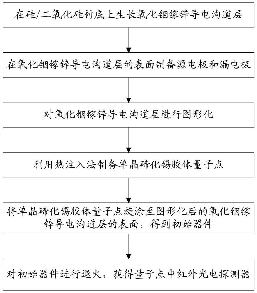
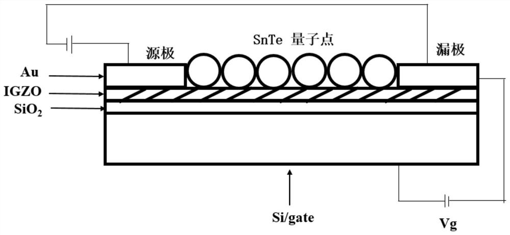
[0048] (1) on Si / SiO 2 Ar / O on the substrate by magnetron sputtering 2An IGZO film with a thickness of about 10-100 nm is grown under a mixed atmosphere. IGZO film is used as the conductive channel layer. The background vacuum reaches 10 -4 ~10 -5 Pa; the pressure in the cavity is 0.7Pa during growth. Anneal the plated IGZO film at 200-500°C to make the carrier mobility reach 9.23m 2 V -1 the s -1 , the on-off ratio is 5×10 7 .

[0049] (2) Prepare source and drain electrodes on the surface of the IGZO film. Specifically, the patterning of the photoresist is realized through the ultraviolet exposure process or the ultraviolet lithography technology, and the Ti / Au composite electrode film is evaporated through the thermal evaporation coating process as the source and drain electrodes. Wherein, the thickness of the Ti film is 5-10 nm, and the thickness of the Au film is 50-200 nm.

[0050] (3) Patterning of the IGZO conductive channel layer. Photoresist patterning is...

Embodiment 2

[0064] (1) on Si / SiO 2 Ar / O on the substrate by magnetron sputtering 2 An IGZO thin film with a thickness of 40nm was grown under the mixed atmosphere. IGZO film is used as the conductive channel layer. The background vacuum reaches 5×10 -4 Pa; the pressure in the cavity is 0.7Pa during growth. The target InGaZn atomic ratio is In:Ga:Zn=2:2:1, and the purity is 99.99%. The plated IGZO film was annealed at 350 °C.

[0065] (2) Prepare source and drain electrodes on the surface of IGZO. The patterning of photoresist is realized by ultraviolet exposure process or ultraviolet lithography technology, and the Ti / Au composite electrode film is evaporated by thermal evaporation coating process as the source and drain electrodes. Wherein, the thickness of the Ti film is 5-10 nm, and the thickness of the Au film is 50-200 nm.

[0066] (3) Patterning of the IGZO conductive channel layer. Photoresist patterning is realized by ultraviolet exposure process, and hydrochloric acid is ...


PUM

PropertyMeasurementUnit
Thicknessaaaaaaaaaa
Concentrationaaaaaaaaaa
Particle sizeaaaaaaaaaa

Abstract

The invention relates to a quantum dot mid-infrared photoelectric detector and a preparation method thereof. The preparation method comprises the following steps: growing an indium gallium zinc oxide conducting channel layer on a silicon/silicon dioxide substrate; preparing a source electrode and a drain electrode on the surface of the indium gallium zinc oxide conductive channel layer; performing patterning on the indium gallium zinc oxide conductive channel layer; preparing single crystal tin telluride colloidal quantum dots by using a thermal injection method; spin-coating the surface of the patterned indium gallium zinc oxide conductive channel layer with the single crystal tin telluride colloid quantum dots to obtain an initial device; and annealing the initial device to obtain the quantum dot mid-infrared photoelectric detector. The quantum dot mid-infrared photoelectric detector prepared by the method can solve the non-toxic problem of the mid-infrared quantum dot material and the problem of widening the response wave band of the quantum dot detector.

Description

technical field [0001] The invention relates to the technical field of photoelectric detection of nanomaterials, in particular to a quantum dot mid-infrared photodetector and a preparation method thereof. Background technique [0002] Quantum dots have the advantages of adjustable bandgap, unique photosensitive and quantum effects, and solution processing. They are one of the core competitive materials for photodetectors, especially uncooled infrared detectors. The response bands of most quantum dot devices are only in the visible and near-infrared, and it is difficult to broaden to the mid-infrared band. Only mercury telluride quantum dot detectors have mid-infrared detection performance. However, due to the high toxicity and instability of mercury telluride, the easy degradation restricts the application range and reliability of mercury telluride quantum dot detectors. Therefore, the development of non-toxic and stable medium-wave quantum dot detectors is a key problem t...

Claims


Application Information

Patent Timeline
IPC IPC(8): H01L31/18H01L31/0296H01L31/0352H01L31/112
CPCH01L31/035218H01L31/02963H01L31/1828H01L31/112Y02P70/50
Inventor 常慧聪冯亚军刘军库郭楠肖林
Owner CHINA ACADEMY OF SPACE TECHNOLOGY
Why Eureka
Try Eureka