Method and system for growing ultra-wide bandgap semiconductor material by ultraviolet-assisted MOCVD (Metal Organic Chemical Vapor Deposition)

A wide-bandgap semiconductor and semiconductor technology, applied in semiconductor/solid-state device manufacturing, metal material coating process, coating, etc., can solve problems such as decomposition or oxidation, enhanced optical absorption of materials, and reduced lifespan

Pending Publication Date: 2022-06-21
NINGBO INST OF MATERIALS TECH & ENG CHINESE ACADEMY OF SCI
View PDF0 Cites 1 Cited by
  • Summary
  • Abstract
  • Description
  • Claims
  • Application Information

AI Technical Summary

Problems solved by technology

However, the shortcomings of traditional MOCVD epitaxial growth of AlN, BN and other ultra-wide bandgap semiconductor materials are: 1) Al, B and other atomic mobility is insufficient, three-dimensional nucleation growth is dominant, threading dislocation density is high, crystal quality and shape At the same time, due to the existence of point defects, the optical absorption of the material is enhanced; 2) With the increase of the bandgap width, the defect state energy level of the ultra-wide bandgap film gradually transitions to the deep energy level, and the crystal point defect concentration is steep Increase, excessive stress will cause cracking problems, and the doping self-compensation effect will be intensified, and the doping ef

Method used


Image

  • Method and system for growing ultra-wide bandgap semiconductor material by ultraviolet-assisted MOCVD (Metal Organic Chemical Vapor Deposition)
  • Method and system for growing ultra-wide bandgap semiconductor material by ultraviolet-assisted MOCVD (Metal Organic Chemical Vapor Deposition)
  • Method and system for growing ultra-wide bandgap semiconductor material by ultraviolet-assisted MOCVD (Metal Organic Chemical Vapor Deposition)

Examples


Embodiment 1

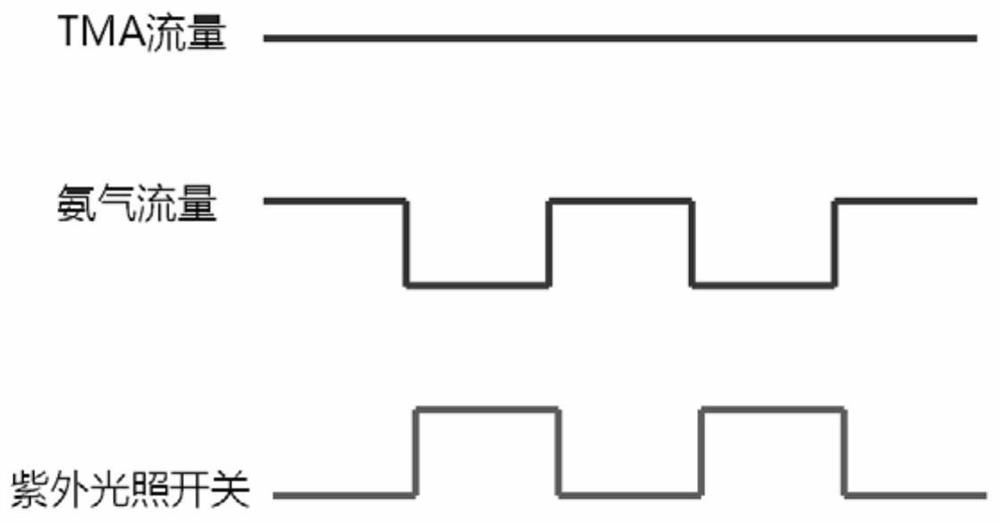
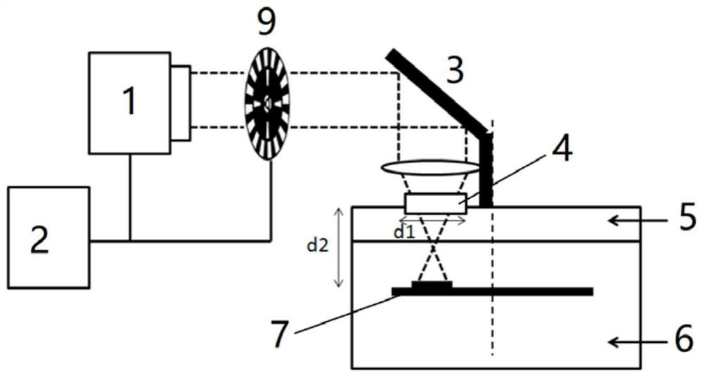
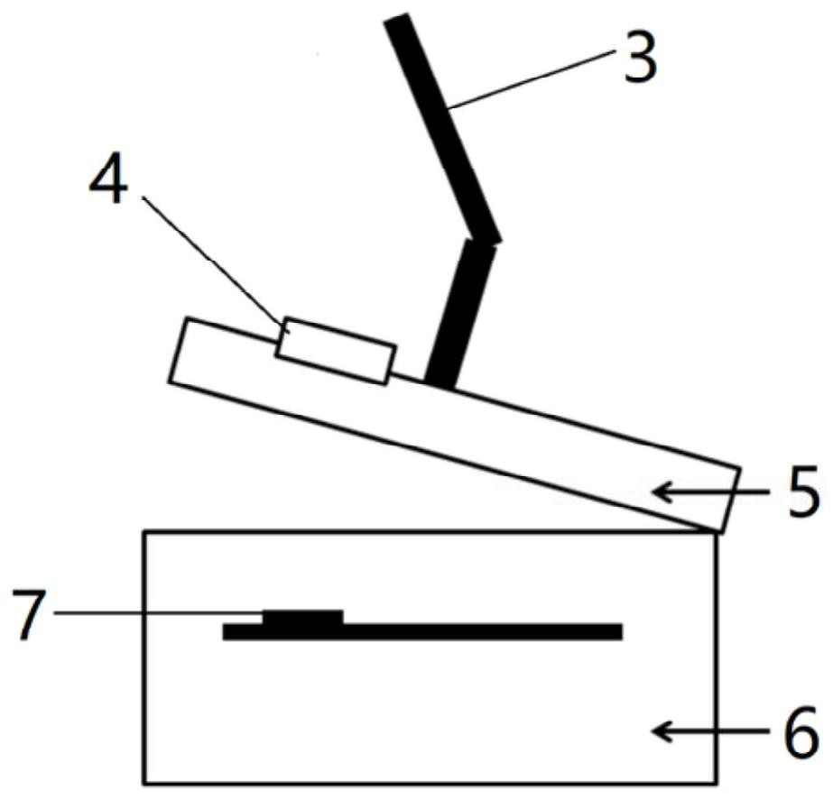
[0078] The process conditions for growing AlN epitaxial film by using this system include: trimethylaluminum (TMA) and ammonia gas are used as gas sources. The carrier gas is H 2 The flow rates of ammonia gas and carrier gas are 1slm and 10slm respectively; the V / III ratio of epitaxial growth is 200; the growth temperature is 1200°C, TMA is fed continuously, and ammonia gas is fed at intervals in a pulsed manner, with an interval of 10s. The duty ratio is 70%; during the interval time when the ammonia gas is not introduced, the surface of the sample is irradiated with ultraviolet light, and a 3 μm AlN epitaxial film is grown.

[0079] In Comparative Example 1 of this embodiment, the method for growing an ultra-wide bandgap semiconductor material is basically the same as that of this embodiment, except that ultraviolet light pulse irradiation is not used.

[0080] In Comparative Example 2 of this embodiment, the method for growing an ultra-wide bandgap semiconductor material i...

Embodiment 2

[0084] Utilizing the technical solutions of the above embodiments of the present application can effectively improve the crystal quality of ultra-wide bandgap semiconductor materials, increase their carrier concentration and electrical breakdown level, and facilitate the growth of thicker ultra-wide bandgap semiconductor materials and ensure It is uniform and complete, and can reduce the difficulty and energy consumption of its manufacturing process.

[0085] It should be noted that in this article, relational terms such as first and second are only used to distinguish one entity or operation from another entity or operation, and do not necessarily require or imply that there is a relationship between these entities or operations. There is no such actual relationship or order between them. Furthermore, the term "comprises", "comprises" or any other variation thereof is intended to cover a non-exclusive inclusion such that a process, method, article, or apparatus comprising a s...


PUM


Abstract

The invention discloses a method and a system for growing an ultra-wide bandgap semiconductor material through ultraviolet-assisted MOCVD (Metal Organic Chemical Vapor Deposition). The method comprises the steps that when the ultra-wide bandgap semiconductor material grows through the MOCVD technology, pulse ultraviolet light evenly irradiates the surface of a substrate or the ultra-wide bandgap semiconductor material growing on the surface of the substrate, the energy of the ultraviolet light is larger than the bandgap width of the ultra-wide bandgap semiconductor material, and the illumination intensity of the ultraviolet light is gt; and 0.2 W/cm < 2 >. By utilizing the technical scheme of the invention, the epitaxial growth process difficulty and energy consumption of the ultra-wide bandgap semiconductor material can be reduced, and the crystal quality, the stress level, the optical transmission performance and the electrical breakdown characteristic of the ultra-wide bandgap semiconductor material can be remarkably improved.

Description

technical field [0001] The present application relates to a method for growing semiconductor materials, in particular to a method and system for growing ultra-wide bandgap semiconductor materials by UV-assisted MOCVD. Background technique [0002] Ultra-wide bandgap semiconductor materials include AlN, high-aluminum components AlGaN, Ga 2 o 3 , BN and other materials. They have the advantages of large band gap, high breakdown electric field, high thermal conductivity, excellent power characteristics at high frequencies, and low energy loss. It has a wide range of applications in the fields of power electronics, microwave radio frequency and ultraviolet optoelectronics. At present, the most important mass production method of wide bandgap semiconductor materials is based on metal organic vapor phase epitaxy deposition equipment (MOCVD). The reaction principle is to perform high-temperature epitaxial growth on substrates such as sapphire, silicon, and silicon carbide, rely...

Claims


Application Information

Patent Timeline
IPC IPC(8): C23C16/18C23C16/48H01L21/02
CPCC23C16/18C23C16/482H01L21/0254H01L21/0262
Inventor 郭炜叶继春
Owner NINGBO INST OF MATERIALS TECH & ENG CHINESE ACADEMY OF SCI
Why Eureka
Try Eureka