Electron-rich negative electrode current collector, preparation method thereof, electrode plate and battery
An electrode pole piece, electron-rich technology, applied in the direction of electrode carrier/current collector, non-aqueous electrolyte battery, non-aqueous electrolyte battery electrode, etc. problems such as rising, to achieve the effect of simple and controllable preparation method, easy industrial production, and small interface resistance
- Summary
- Abstract
- Description
- Claims
- Application Information
AI Technical Summary
Problems solved by technology
Method used
Image
Examples
preparation example Construction
[0048] Another aspect of the present invention also provides a method for preparing the aforementioned electron-rich negative electrode current collector, comprising the following steps:
[0049] A polymer base material layer is provided, and electron-rich copper nanoparticles are plated on both sides of the polymer base material layer by vacuum magnetron sputtering to obtain two nano-copper layers;
[0050] Wherein, the preparation method of electron-rich copper nanoparticles comprises the following steps:
[0051] will [Gd 2 C] 2+ ·2e - The electret, divalent copper salt and alcohol solvent are mixed and reacted at 60℃~120℃, and then [Gd 2 C] 2+ ·2e - Electret adsorption, transfer the remaining reaction system and carry out solid-liquid separation, collect the solid phase and dry. Preferably, the magnetic substance is a magnet.
[0052] By adding [Gd 2 C] 2+ ·2e - Electron-rich copper nanoparticles are prepared from electrets and divalent copper salt precursors thr...
Embodiment 1
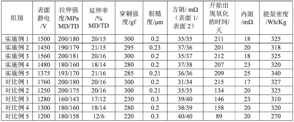
[0071] (1) 1 mmol of [Gd 2 C] 2+ ·2e - The electret, 0.5 mmol of copper chloride and 5 mL of hexanol were mixed, reacted at 80 °C for 50 min, and then the [Gd 2 C] 2+ ·2e - electret adsorption, the remaining reaction system is subjected to solid-liquid separation, the solid phase is collected and dried to obtain copper nanoparticles with an average particle size of 30 nm;
[0072] (2) The copper nanoparticles obtained in step (1) were prepared as a target, fixed on the cathode of the magnetron sputtering apparatus, and a 4 μm thick polyethylene terephthalate substrate layer (weight average molecular weight 100000 Da) was , surface roughness 150nm) placed on the anode of the magnetron sputtering apparatus; vacuum the magnetron sputtering apparatus to a degree of vacuum ≤5×10 -2 After Pa, fill with 10Pa argon gas, and then apply a voltage of 3000V between the cathode and the anode, so that the atoms in the target fly to the anode under the action of the electric field, on o...
Embodiment 2
[0075] It is basically the same as Example 1, except that the reaction temperature in step (1) is adjusted to be 60° C., so that the average particle size of the copper nanoparticles is 45 nm.
PUM
| Property | Measurement | Unit |
|---|---|---|
| particle diameter | aaaaa | aaaaa |
| surface roughness | aaaaa | aaaaa |
| molecular weight | aaaaa | aaaaa |
Abstract
Description
Claims
Application Information
