Copper-indium-galliun-selenium film solar cell and its preparation method

A technology for solar cells and copper indium gallium selenide, which is applied to circuits, photovoltaic power generation, electrical components, etc., can solve the problems of increasing the technological process and increasing the production cost, and achieves the effects of simple battery structure, improved production yield and simple process.

Inactive Publication Date: 2002-09-04
TSINGHUA UNIV
View PDF5 Cites 44 Cited by
  • Summary
  • Abstract
  • Description
  • Claims
  • Application Information

AI Technical Summary

Problems solved by technology

[0004] In addition, the back electrode of the battery is generally made of metal molybdenum, such as the back electrode of the CIGS thin film solar cell in patent US3978510, patent US4465575 and patent US4335266. Patent WO 97 / 22152 reports that a metal copper layer is coated on the molybdenum layer by electrodeposition to make a metal composite layer as the back electrode, but this increases the process and increases the production cost

Method used


Image

  • Copper-indium-galliun-selenium film solar cell and its preparation method
  • Copper-indium-galliun-selenium film solar cell and its preparation method
  • Copper-indium-galliun-selenium film solar cell and its preparation method

Examples


preparation example Construction

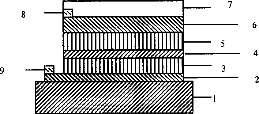
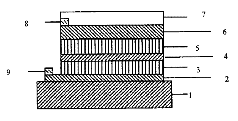
[0025] The preparation method of the ZnS window layer 5 may be electroless plating or vacuum evaporation. Among them, electroless plating can be selected to contain Zn +2 (0.1-0.3M), ammonia water (5-8M, PH=10.5-11.0), thiourea (NH 2 CSNH 2 , 0.3-0.9M) bath, temperature at 60-85 ° C, electroless ZnS layer. Among them, the vacuum evaporation method can choose ZnS crystal particles, which can be realized by thermal evaporation or electron beam evaporation. The film thickness is 70-220nm.

[0026]The transparent electrode 6 can be selected from zinc aluminum oxide (ZAO) or indium tin oxide (ITO), etc., wherein the preparation method of zinc aluminum oxide can use metal target sputtering, and the zinc aluminum oxide thin film with the best performance is made of zinc aluminum oxide ceramic target Prepared by radio frequency or high frequency AC magnetron sputtering. The thickness of this layer is 0.10-0.35 μm. ITO is generally prepared by magnetron sputtering using ceramic t...

Embodiment 1

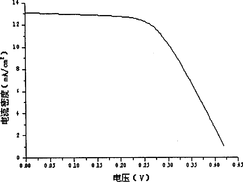
[0029] On the surface of soda-lime glass, a Cu-Mo alloy back electrode was deposited by sputtering with Cu and Mo alloy targets, with a thickness of about 1.45 μm. The content of Cu in the prepared Cu-Mo alloy film was 6%. Then, the co-evaporation method is used, that is, Cu, In, Ga, Se are used for reactive evaporation to form Cu(In, Ga)Se on the substrate. 2 The thin film starts to evaporate sulfur when its thickness grows to 2.0 μm. The substrate temperature is 350°C, and the evaporation rate is 6 / S. A sulfur-containing preliminary layer was formed with a thickness of about 50 nm. Then, under an argon protective atmosphere, annealing is performed at 500° C. for 15 minutes to form a CIGSS thin film. After cleaning and drying with argon, immerse at room temperature containing 0.1MZn +2 , 7M ammonia water, 0.6M thiourea solution, take it out after 30 seconds, raise the temperature of the plating solution to 85°C, and dip it repeatedly five times to form a dense ZnS film lay...

Embodiment 2

[0031] On the surface of soda-lime glass, a Cu-Mo alloy back electrode was deposited by sputtering with Cu and Mo alloy targets, with a thickness of about 1.45 μm. The content of Cu in the prepared Cu-Mo alloy film was 15%. After cleaning and drying with argon gas, a preliminary layer containing Cu, In and Ga was formed on the substrate by magnetron sputtering, and its thickness was 1.2 μm. On its surface, a selenium layer with a thickness of 0.7 μm was evaporated, and kept at 500° C. for 20 minutes in an atmosphere of selenium. Subsequently, co-evaporation of sulfur and indium is carried out. The substrate temperature is 450° C., and after vacuum annealing at 500° C. for 10 minutes, a CIGSS film with a thickness of about 35 nm is formed. Immerse at room temperature containing 0.2MZn +2 , 6M ammonia water, 0.8M thiourea solution, take it out after 30 seconds, raise the temperature of the plating solution to 80°C, and dip it five times repeatedly to form a dense ZnS thin film...


PUM


Abstract

A film solar battery with copper, indium, gallium selenium and its parparing method relates to semiconductor film preparation and structure design of semiconductor film device. It has the characteristics as using n-ZnS as a window layer, CuIn GaSe P-semiconductor film as an absorption layer and to form ZnS/Cu (In,Ga) Sezp-n junction with ZnS, of which metal back electrode is Mo-Cu alloy. In present invention. ZnS has been used as a window layer of film solar battery to replace ZnO material so as to increase absorption spectral region of sun light at absorption layer and to avoid the application of hazardous material of Cd, furthermore Mo-Cu alloy has been used as a back electrode to replace Mo for making joint between battery and backing more solid to raise the yield of battery production.

Description

technical field [0001] The invention belongs to the technical field of optoelectronic materials and new energy, and relates to the preparation of semiconductor thin films and the structural design of semiconductor thin film devices, in particular to the structural design and preparation method of thin-film solar cells using copper indium gallium selenium thin films as absorbing layers. Background technique [0002] The compound semiconductor copper indium selenide (CuInSe) with chalcopyrite structure 2 , referred to as CIS) or copper indium gallium selenide (Cu(In,Ga)Se) with gallium in solid solution 2 , referred to as CIGS) film as a light-absorbing layer of thin-film solar cells not only has high energy conversion efficiency, but also has radiation stability, and thus become one of the research hotspots in the field of photovoltaic cells. Copper indium gallium selenide (CIGS) solar cells are photovoltaic devices formed by depositing multi-layer thin films on glass or oth...

Claims


Application Information

Patent Timeline
Patent Type & Authority Applications(China)
IPC IPC(8): H01L31/0224H01L31/054H01L31/18
CPCY02E10/52Y02P70/50
Inventor 庄大明张弓方玲杨波
Owner TSINGHUA UNIV
Why Eureka
Try Eureka