
Adhesive sheet for semiconductor connecting substrate, adhesive-backed tape for TAB, adhesive-backed tape for wire bonding connection, semiconductor connecting substrate, and semiconductor device

a technology for connecting substrates and adhesives, applied in the direction of heat-activated film/foil adhesives, film/foil adhesives, transportation and packaging, etc., can solve the problems of high adhesive strength not allowing peeling, especially difficult to achieve a balance between adhesive strength and adhesive strength, and the inability to achieve total satisfactory properties

Inactive Publication Date: 2002-02-28
TORAY IND INC
View PDF0 Cites 19 Cited by
  • Summary
  • Abstract
  • Description
  • Claims
  • Application Information

AI Technical Summary

Benefits of technology

[0019] (b) Moderate elastic modulus and moderate coefficient of linear expansion to ease the thermal stress acting on the different materials forming the connecting substrate due to temperature cycles and reflow.
[0129] The phenol resins which can be used here include those publicly known such as novolak type phenol resins and resol type phenol resins, for example, resins of phenol, alkyl substituted phenols such as cresol, p-t-butylphenol, nonylphenol and p-phenylphenol, and of cyclic alkyl modified phenols such as terpene and dicyclopentadiene, resins with functional groups containing a hetero atom such as nitro groups, halogen groups, cyano groups and amino groups, resins with a skeleton of naphthalene, anthracene, etc., and resins of polyfunctional phenols such as bisphenol F, bisphenol A, bisphenol S, resorcinol and pyrogallol. Among them, a resol type phenol resin is more suitable since it is effective in improving the insulation resistance dropping time.

Problems solved by technology

(a) High adhesive strength not allowing peeling even at a reflow temperature of 230.degree. C. or higher.
(b) Moderate elastic modulus and moderate coefficient of linear expansion to ease the thermal stress acting on the different materials forming the connecting substrate due to temperature cycles and reflow.
(c) Processability to allow sticking together and low temperature short time thermal cure.
(d) Insulatability in lamination on wiring.
Of the above properties, it has been especially difficult to achieve a balance between adhesive strength on the one hand and moderate elastic modulus and coefficient of linear expansion on the other hand.
In the conventional adhesive compositions, if the adhesive strength is attempted to be improved, the elastic modulus at high temperature drops to pose a problem that totally satisfactory properties cannot be obtained.
In general, the adhesive strength of an adhesive can be enhanced by lowering the elastic modulus to increase the breaking energy, but this method presents a problem in that at high temperature and high humidity, the adhesive is softened, to lower the reflow resistance as well as the adhesive strength at high temperature and high humidity.
On the other hand, if the crosslinking degree of the adhesive is increased to improve the reflow resistance and the adhesive strength at high temperature and high humidity, the adhesive is likely to cause brittle fracture, and the internal stress due to curing shrinkage increases, to unpreferably lower the adhesive strength on the contrary.
Furthermore, the effect for easing the thermal stress caused by temperature difference is also lost.
However, in the above mentioned insulation reliability and adhesive strength, the conventional tapes for TAB are not satisfactory enough.
For example, since the insulation drops fast when a voltage is applied continuously at high temperature and high humidity, the insulation reliability is insufficient.
Especially when the calorific value is large in an integrated circuit acting at a high speed, etc., a serious accident can happen.
Furthermore, since the adhesive strength is low, it can happen that conductors peel during pattern processing or that the inner leads peculiar to the TAB method are peeled, not allowing production.
Furthermore, the said tape for WB presents the following problems.
Furthermore, in the WB method, it can happen that the heating and ultrasonic wave application at the time of wire bonding soften the adhesive layer, not allowing wire bonding.
However, in the above mentioned insulation reliability, adhesive strength and WB property, the conventional tapes for WB cannot be said to be satisfactory enough.
For example, if the adhesive strength to the conductor is enhanced, the insulation with a voltage applied continuously at high temperature and high humidity drops fast, to show insufficient insulation reliability, and the WB property also drops.
On the other hand, if the heat resistance is enhanced to improve the insulation reliability and WB property, the adhesive strength drops, causing the conductor to peel during pattern processing and also after completion of WB.
If the storage elastic modulus is less than 0.1 MPa, the strength of the adhesive is so low that when an apparatus mounted with the IC package is used, the semiconductor connecting substrate is deformed and that when the adhesive sheet is processed, it is unpreferably poor in handling convenience.
If more than 10000 MPa, the effect of easing the thermal stress is so low as to unpreferably cause warping of the semiconductor connecting substrate, peeling of the respective layers and cracking of solder balls.
If the amine value is less than 1, the effect of enhancing insulatability and adhesive strength is too small, and if more than 3, the curing reaction progresses excessively to unpreferably lower processability.
If the amount of the thermosetting resin added is less than 5 parts by weight, it is not preferable because the elastic modulus at high temperature drops so remarkably that the semiconductor integrated circuit connecting substrate is deformed while using the apparatus on which the semiconductor device is mounted, and that the handling convenience during processing is poor.
If the amount of the thermosetting resin used exceeds 400 parts by weight, the elastic modulus is so high that the coefficient of linear expansion becomes small, to unpreferably lower the effect of easing the thermal stress.
If higher than 110.degree. C., the difference from the copper foil or insulating base film in the coefficient of linear expansion cannot be absorbed, and warping is caused, to unpreferably lower the dimensional accuracy.
However, in this case, hard and fragile properties are caused at room temperature, and a drop of adhesive strength to the copper foil and the drop of flexibility occur.
The reason is considered to be that the compatibility between the thermosetting resin and the thermoplastic resin is not appropriate.
If the haze is less than 8, the compatibility is too good, and it is unpreferable because only average properties as a simple mixture can be obtained.
If more than 45, the mixture is too heterogeneous, and the properties of either ingredient are unpreferably manifested too strongly.

Method used


Image

  • Adhesive sheet for semiconductor connecting substrate, adhesive-backed tape for TAB, adhesive-backed tape for wire bonding connection, semiconductor connecting substrate, and semiconductor device
  • Adhesive sheet for semiconductor connecting substrate, adhesive-backed tape for TAB, adhesive-backed tape for wire bonding connection, semiconductor connecting substrate, and semiconductor device
  • Adhesive sheet for semiconductor connecting substrate, adhesive-backed tape for TAB, adhesive-backed tape for wire bonding connection, semiconductor connecting substrate, and semiconductor device

Examples


example 2

[0183] Spherical silica ("Ecserica" produced by Tokuyama Corp.) was mixed with toluene, and the mixture was treated by a sand mill, to prepare a dispersion. NBR-C (PNR-1H produced by Japan Synthetic Rubber Co., Ltd.), SEBS-C (Mx-073 produced by Asahi Chemical Industry Co., Ltd.), naphthalene skeleton-containing epoxy resin ("Epiclon" HP4032 produced by Danippon Ink & Chemicals, Inc., 150 in epoxy equivalent), 4,4'-diaminodiphenylsulfone, and methyl ethyl ketone equal in weight to the dispersion were added to the dispersion to achieve the composition ratio shown in Table 1, and the mixture was stirred at 30.degree. C. to prepare an adhesive solution. The adhesive solution was used to obtain a pure copper sheet with an adhesive layer as described in Example 1. The properties are shown in Table 3.

examples 3 to 6

[0184] Adhesives prepared by using the raw materials shown in Table 1 at the composition ratios shown in Table 2 as described in Example 1 were used to obtain adhesive sheets for semiconduction connecting substrates. The properties are also shown in Table 3.

example 7

[0190] The polyamide resin (2.5 in amine value) obtained in Reference Example 1, epoxy resin ("Epiclon" HP4032 produced by Dainippon Ink & Chemicals, Inc., 150 in epoxy equivalent), nonylphenol type resol phenol resin (CRM0803 produced by Showa High polymer Co., Ltd.), straight type phenol resol resin (PR50087 produced by Sumitomo Durez Co., Ltd.), p-t-Bu / bisphenol A mixed type (p-t-Bu / bisphenol A=8 / 2) phenol resol resin (CKM935 produced by Showa High polymer Co., Ltd.) and DBU were mixed to achieve the composition ratio shown in Table 2, and the mixture was stirred in a mixed solvent of methanol and monochlorobenzene at 30.degree. C., to achieve a concentration of 20 wt. %, for preparing an adhesive solution. The adhesive was applied by a bar coater, to a 25 .mu. thick polyethylene terephthalate film ("Lumirror" produced by Toray Industries, Inc.) used as a protective film, to achieve a dry thickness of about 12 .mu., and the laminate was dried at 100.degree. C. for 1 minute and at...


PUM

PropertyMeasurementUnit
temperatureaaaaaaaaaa
storage elastic modulusaaaaaaaaaa
RHaaaaaaaaaa

Abstract

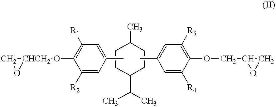
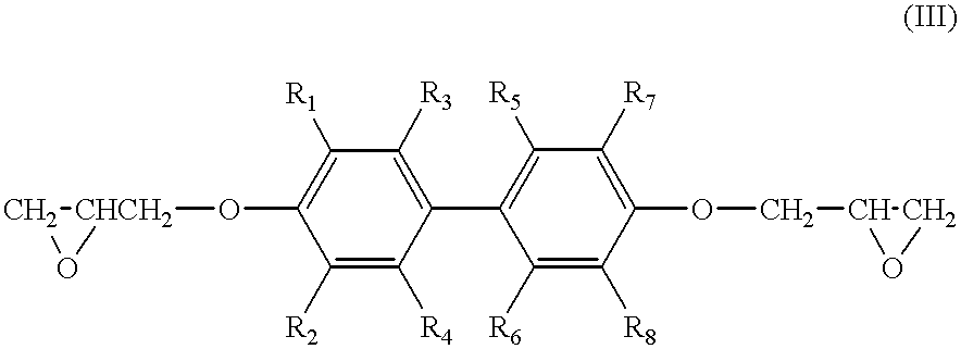
An adhesive sheet for a semiconductor connecting substrate consisting of a laminate having an adhesive layer on a substrate, wherein said adhesive layer contains a thermoplastic resin (A) and an epoxy resin (B) and said epoxy resin (B) contains at least one epoxy resin (B) selected from (I) dicyclopentadiene skeleton-containing epoxy resins, (II) terpene skeleton-containing epoxy resins, and (III) biphenyl skeleton-containing epoxy resins, as an essential component; an adhesive-backed tape for TAB consisting of a laminate having an adhesive layer and a protective film layer on a flexible organic insulating film. The adhesive sheet for a semiconductor connecting substrate, the adhesive-backed tape for TAB and the adhesive-backed tape for wire bonding connection of the present invention are excellent in adhesive strength, insulatability, dimensional accuracy, etc., and can improve the reliability of a semiconductor integrated circuit connecting substrate and a semiconductor device respectively for high density packaging.

Description

[0001] The present invention relates to an adhesive sheet suitable as an adhesive layer for a semiconductor connecting substrate used for mounting a semiconductor integrated circuit, an adhesive-backed tape used for tape automated bonding (TAB) (hereinafter called "a tape for TAB"), an adhesive-backed tape used for wire bonding connection (hereinafter called "a tape for WB"), and a semiconductor connecting substrate and a semiconductor device using any of the foregoing.BACKGROUND ARTS[0002] Conventional semiconductor integrated circuit (IC) mounting techniques include the following.[0003] For mounting an IC, a method in which the electrodes of the IC are wire-bonded to metallic lead frames and sealed by a resin is most popularly used. IC packages produced in this manner are usually provided in such forms as the small outline package (SOP) and the quad flat package (QFP). In contrast to these, as smaller-sized and lighter-weight electronic apparatuses, a ball grid array (BGA), in whi...

Claims


Application Information

Patent Timeline
Patent Type & Authority Applications(United States)
IPC IPC(8): C08G59/24C08L55/00C08L77/00C09J7/22C09J7/35C09J163/00H01L23/495H01L23/498
CPCC08G59/245Y10T428/2826C08L77/00C09J7/0242C09J163/00C09J2203/326C09J2463/00H01L23/49572H01L23/49816H01L24/50H01L2224/16H01L2224/48095H01L2924/01005H01L2924/01012H01L2924/01013H01L2924/01015H01L2924/0102H01L2924/01027H01L2924/01029H01L2924/0103H01L2924/01033H01L2924/0104H01L2924/01051H01L2924/01078H01L2924/01079H01L2924/01082H01L2924/04953H01L2924/09701H01L2924/14H01L2924/15153H01L2924/1517H01L2924/15311H01L2924/3025C08L55/00Y10T428/287Y10T428/28Y10T428/2883Y10T428/2848H01L2924/07802H01L2224/73265H01L2224/48465H01L24/45H01L2224/45144H01L2924/01047H01L24/48H01L2924/01006H01L2924/01019H01L2924/01023H01L2924/01024H01L2924/01045C08L2666/02H01L2924/00014H01L2924/00H01L2924/351H01L2224/05573H01L2224/05568H01L2924/181C09J7/35C09J7/22H01L24/86Y10T428/31511H01L2924/00012H01L21/76
Inventor SAWAMURA, YASUSHIKIGOSHI, SHOJIHATANO, TAKUKONISHI, YUKITSUNAANDO, YOSHIO
Owner TORAY IND INC
Learn More