

Patterned wafer inspection method and apparatus therefor
a technology of patterned wafers and inspection methods, applied in the direction of semiconductor/solid-state device testing/measurement, instruments, etc., can solve the problems of limiting the inspection time, limiting the high speed, and shortening the inspection tim
- Summary
- Abstract
- Description
- Claims
- Application Information
AI Technical Summary
Benefits of technology
Problems solved by technology
Method used
Image

Examples
embodiment 2
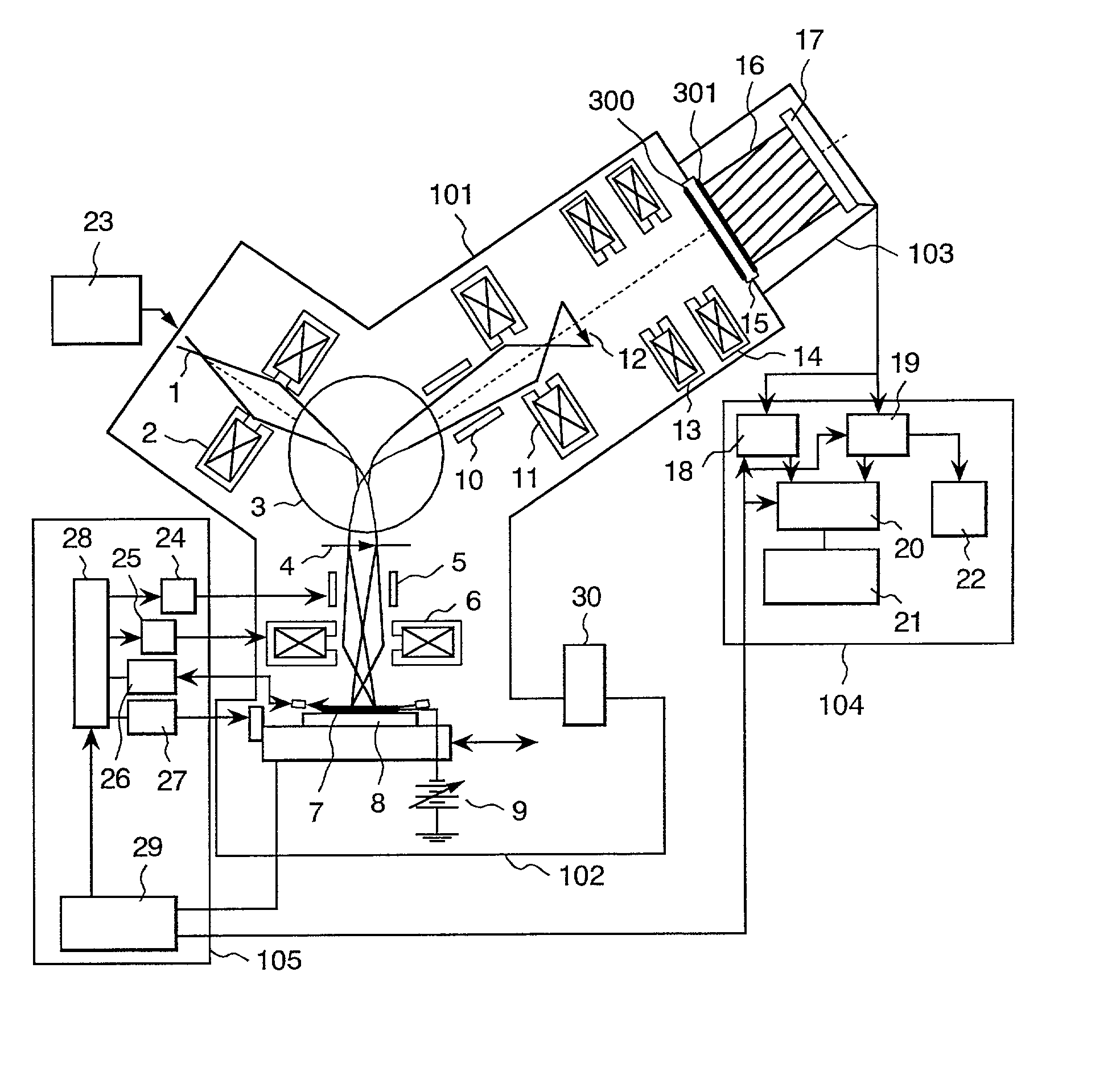
[0054] In the aforementioned Embodiment 1, the area of the electron beam irradiation region of 1 shot is considerably large such as 100 .mu.m.times.100 .mu.m, so that a problem may arise that a distortion is generated in the periphery of the enlarged image of the semiconductor sample or that the beam current density in the irradiation region becomes ununiform. When an image distortion or ununiformity of current density is fixedly generated, it can be corrected by changing the fiber strand layout of the optical fiber bundle 16. The obtaining sensitivity of an image signal and weighting of the image process can be corrected. However, if they vary in time, it is hard to handle by those methods. In this embodiment, the irradiation region of 1 shot is a square of 5 .mu.m and it is designed to prevent the problems of distortion and ununiformity of current density. The irradiation electron beam current is 5 .mu.A per 1 shot. In this case, assuming the electron scattering efficiency .eta. a...
embodiment 3
[0060] In this embodiment, as a device for converting a sample surface image to an electric signal, a time accumulative CCD sensor is used. This sensor is called a TDI sensor and generally used in an optical inspecting apparatus. The constitution other than it is the same as that of the aforementioned Embodiment 2. The operation concept of the TDI sensor will be explained by referring to FIG. 5. The TDI sensor operates so as to move the charge generated according to the intensity of the light received by each light receiving region to the line in the x direction and sequentially add the charge generated according to the intensity of the light received by the moving destination at the same time. Upon arrival at the last line of the light receiving surface, the TDI sensor outputs it to the outside as an electric signal. Therefore, when the moving speed of the charge in the x direction is made equal to the moving speed of an image on the light receiving surface in the x direction, a si...
embodiment 4
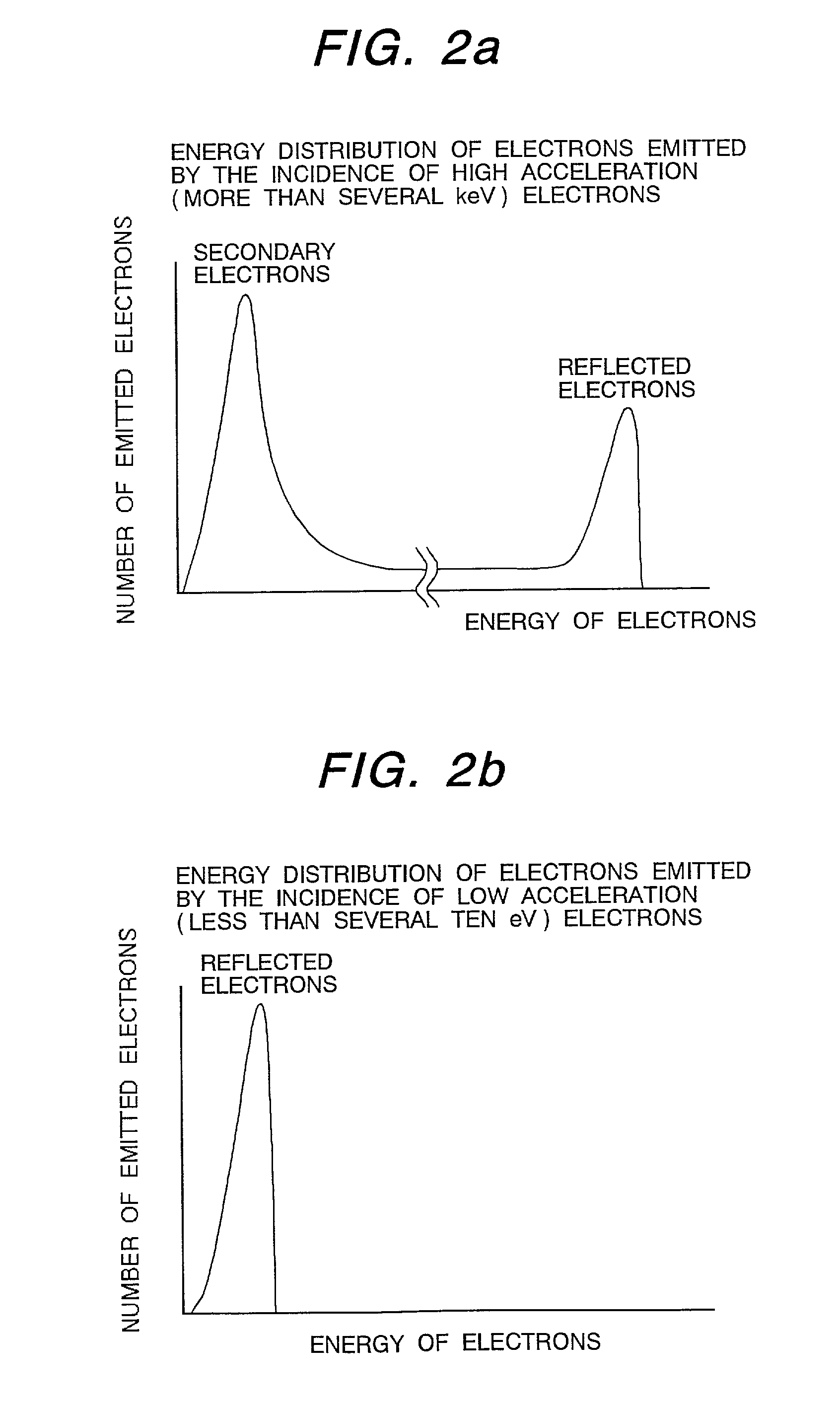
[0063] In the aforementioned Embodiments 1 to 3, a decelerated electron beam is irradiated onto the surface of a semiconductor sample. However, in this embodiment, so as to allow an electron beam to reflect immediately before the surface of a sample without entering the sample surface, a negative potential slightly higher than the acceleration voltage of the electron beam is applied to the sample surface. To form a surface image of the sample, the electron beam reflected immediately before the sample is used. The constitution other than it is exactly the same as that of the aforementioned Embodiment 1. Recently, the surface grinding process such as CMP or CML has been introduced into the semiconductor process and there is a trend that the uneven surface of a semiconductor sample is flattened. In this embodiment, fine irregularities of the surface after such a flattening process can be detected with high sensitivity compared with the aforementioned Embodiment 1. Namely, the character...
PUM
| Property | Measurement | Unit |
|---|---|---|
| area | aaaaa | aaaaa |
| size | aaaaa | aaaaa |
| diameter | aaaaa | aaaaa |
Abstract
Description
Claims
Application Information