Method for making optical device structures

a technology of optical devices and structures, applied in the field of forming optical device structures, can solve the problems of waveguide structures, light transmission losses, difficult to fabricate mirrors with conventional methods,

Inactive Publication Date: 2004-05-27
GENERAL ELECTRIC CO
View PDF2 Cites 22 Cited by
  • Summary
  • Abstract
  • Description
  • Claims
  • Application Information

AI Technical Summary

Benefits of technology

0049] The methods described above can be used to define optical device structures, such as mirrors, waveguides, and lens components. The process enables the formation of waveguide structures with controlled refractive index and smooth, tapered edges to allow vertical interconnection between the electronic portion of the electro-optic modules and the optical bench portion, or vertical connection between the fiber optic cables and the optical bench. Furthermore, the optical device structures describ

Problems solved by technology

This mirror is difficult to fabricate with conventional methods for several reasons.
Another problem encountered with planar polymer waveguides is the necessity to have smooth edges on the waveguide structures to limit l

Method used


Image

  • Method for making optical device structures
  • Method for making optical device structures
  • Method for making optical device structures

Examples


example 1

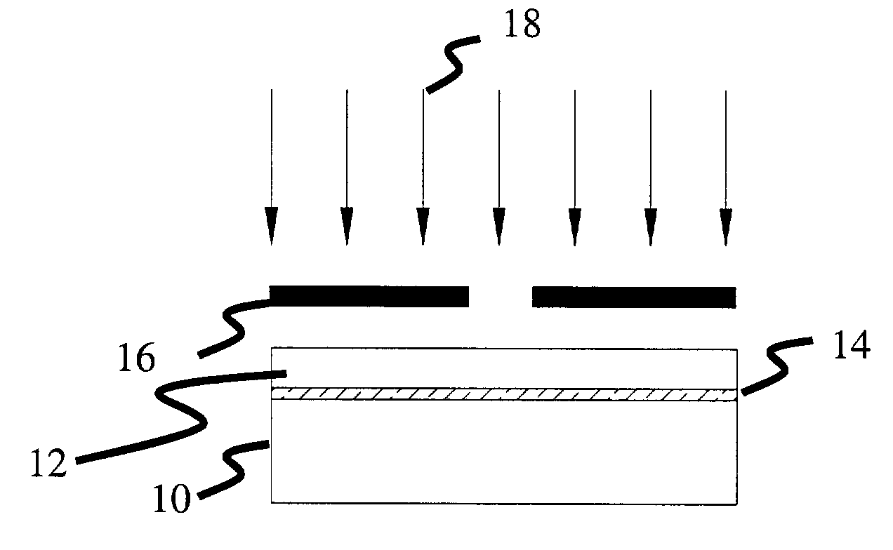
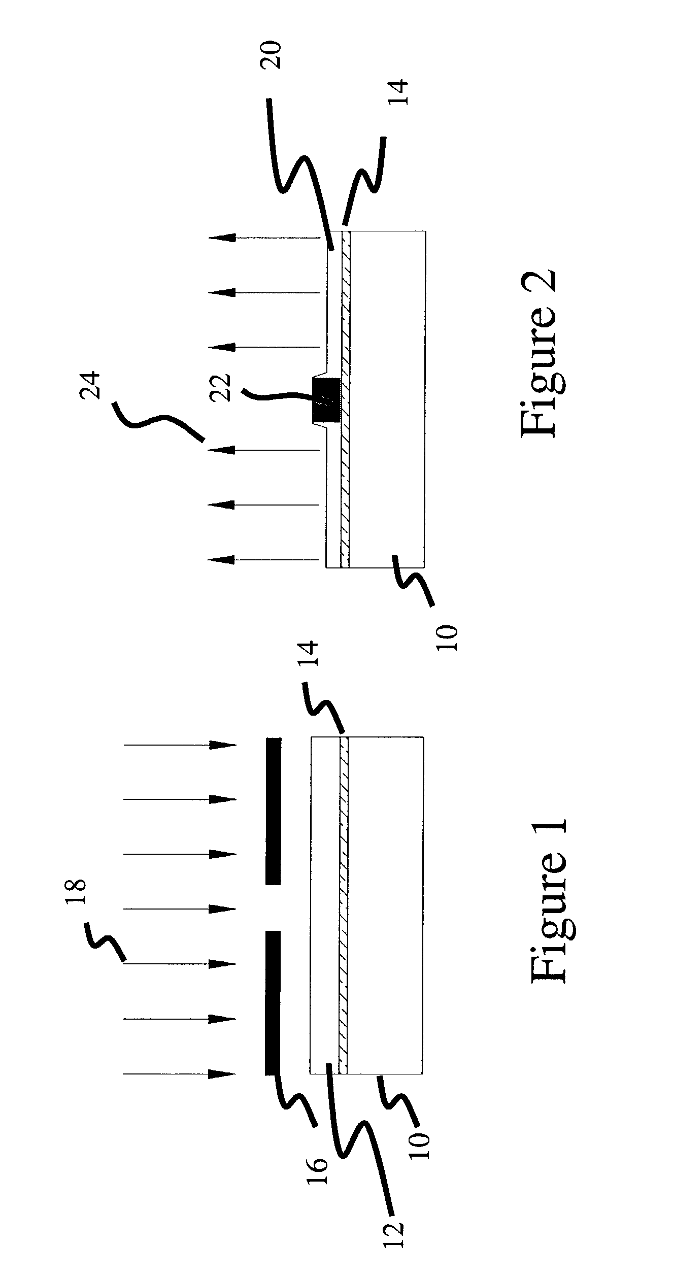
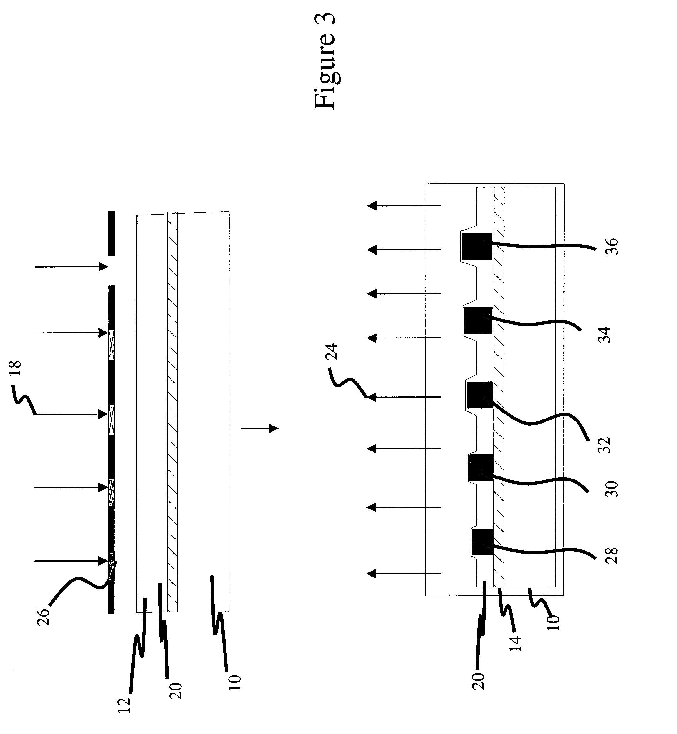
[0052] Example 1 describes the preparation of a surface topography comprising a polymeric composite material derived from Udel polysulfone and CY 179 using UV-irradiation.

[0053] Into a suitable clean glass container, 60 grams of low color grade polysulfone polymer (Udel P-3703, available from Solvay Advanced Polymers, Alpharetta, Ga.) was added along with 210 grams of anhydrous anisole. The blend was warmed to about 50.degree. C. and mixed for about 24 hours to dissolve the polymer. To this mixture was added 20 grams of CY179 epoxy monomer, 0.5 gram of Cyracure UVI-6976, and 0.3 gram of Irganox 1010. The mixture was blended to completely intermix all components and filtered prior to use through a nominal 0.5 micron membrane filter to give the polymerizable composite. A 5 micron thick film of the polymerizable composite was prepared on a glass substrate by spin coating the material at 3000 revolutions per minute (rpm) for 30 seconds and heating on a hotplate for 5 minutes at 80.degre...

example 2

[0054] This Example describes the preparation of a surface topography comprising a polymeric composite material derived from an acrylate copolymer containing about 75% by weight of poly(methyl methacrylate) and 25% poly(tetrafluoropropyl methacrylate) and CY 179 using UV-irradiation.

[0055] Into a glass container, capable of being sealed under vacuum, was distilled 19 grams of tetrafluoropropyl methacrylate, followed by addition of 56 grams of methyl methacrylate, 93 grams of cyclohexanone, 0.15 gram of N-dodecanethiol, and 0.19 gram of benzoyl peroxide. The mixture was degassed and sealed under vacuum. After being heated with mixing at about 75.degree. C. for about 24 hours, followed by further heating at about 80.degree. C. for about 24 hours, the resulting mixture was cooled and treated with 55.5 grams of anisole. The resulting blend was a viscous, clear, and colorless acrylate copolymer consisting of about 75% poly(methyl methacrylate) and 25% poly(tetrafluoropropyl methacrylate)...


PUM


Abstract

A method of forming an optical device structure having a first region and a second region. The method comprises: providing a polymerizable composite comprising a polymer binder and an uncured monomer, depositing the polymerizable composite on a substrate to form a layer, patterning the layer to define an exposed area and an unexposed area of the layer, irradiating the exposed area of layer, and volatilizing the uncured monomer to form the optical device structure. The step of volatilizing the uncured monomer forms a surface topography and a compositional change between the first region and the second region. The compositional change creates a gradient in refractive index between the first region and the second region.

Description

BACKGROUND OF INVENTION[0001] The invention relates to a method of forming an optical device structure comprising an organic polymer composite. More particularly, the present invention relates to a method of forming a topographic profile in an optical device structure. The invention can be used for forming an optical device structure comprising a clad and a core layer.[0002] Modern high-speed communications systems are increasingly using optical fibers for transmitting and receiving high-bandwidth data. The excellent properties of polymer optical fibers with respect to flexibility, ease of handling and installation are an important driving force for their implementation in high bandwidth, short-haul data transmission applications such as fiber to the home, local area networks, and automotive information, diagnostic, and entertainment systems.[0003] In any type of optical communication system there is the need for interconnecting different discrete components. These components may in...

Claims


Application Information

Patent Timeline
IPC IPC(8): G02B3/00G02B6/138G03F7/00G03F7/36G03F7/40
CPCG02B3/0056G02B6/138G03F7/40G03F7/001G03F7/36G03F7/0005G03F1/50
Inventor GORCZYCA, THOMAS BERT
Owner GENERAL ELECTRIC CO
Why Eureka
Try Eureka