

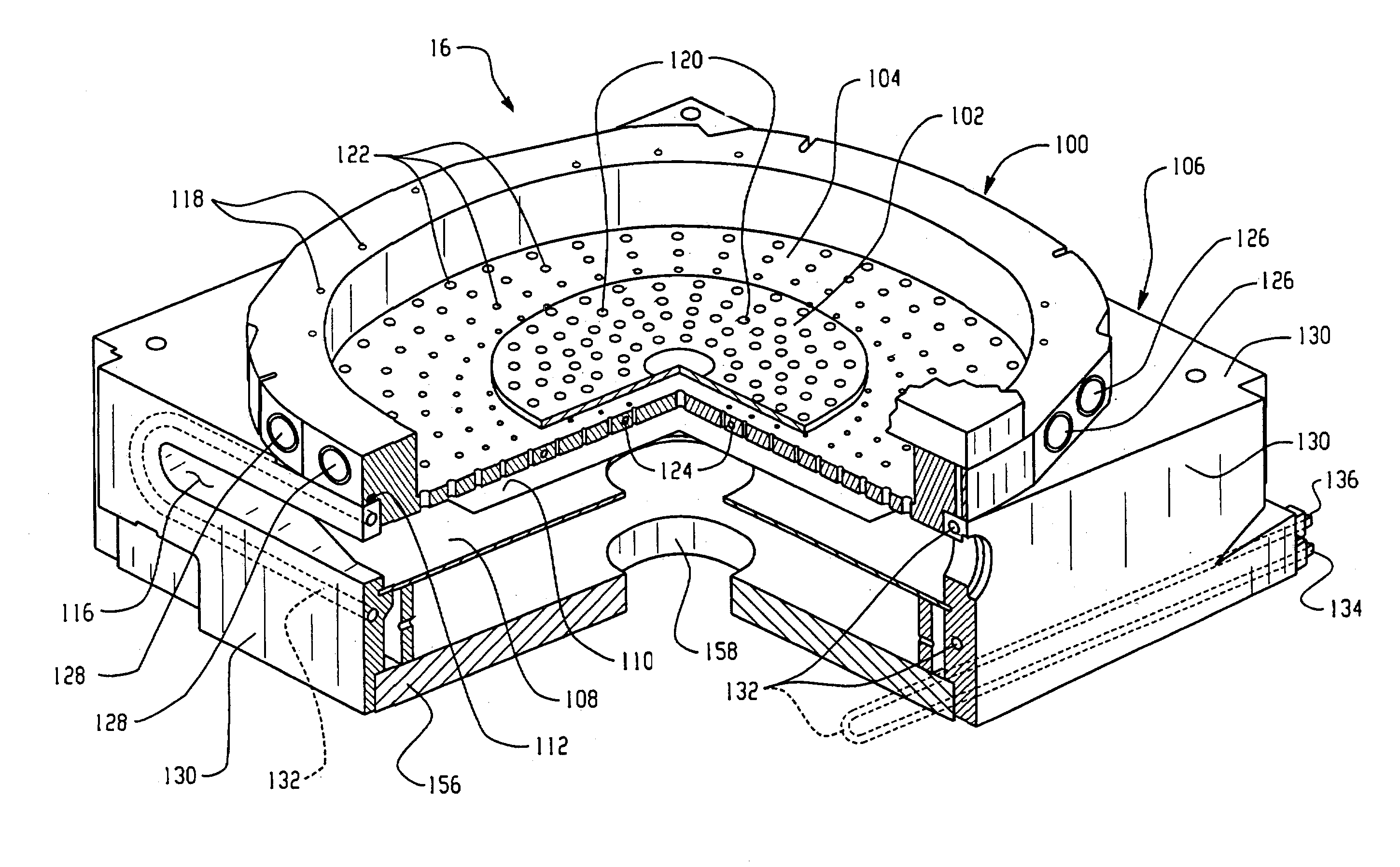
Plasma ashing apparatus and endpoint detection process
a technology of endpoint detection and plasma ashing, which is applied in the direction of photomechanical treatment, instruments, electric discharge tubes, etc., can solve the problems of limiting the overall chip speed, increasing the dielectric constant, and material loss, so as to improve the removal effect of photoresist, reduce the impact area, and flexible the effect of the process platform
- Summary
- Abstract
- Description
- Claims
- Application Information
AI Technical Summary
Benefits of technology
Problems solved by technology
Method used
Image

Examples
example 2
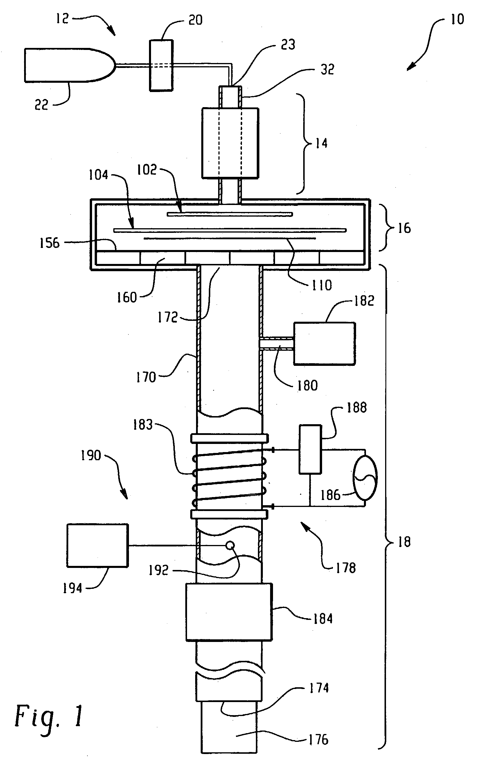
[0082] In this example, CO.sub.2 was monitored in an exhaust conduit of a plasma asher apparatus as shown in FIG. 1. CO.sub.2 was monitored by a residual gas analyzer with and without plasma formed by an afterburner disposed in the exhaust conduit. Similar to Example 1, a resist coated wafer was slowly heated to 300.degree. C. in the process chamber without exposure to plasma. Helium was introduced into the plasma apparatus at a flow rate of 7,000 sccm and at a pressure of 1.5 torr. During operation of the afterburner at an RF power of 300 W, oxygen gas was introduced into the exhaust conduit at a flow rate of 1,000 sccm. No oxygen was introduced into the process chamber. FIG. 10 graphically illustrates CO.sub.2 generation as a function of time resulting from generating plasma in the exhaust conduit. If the afterburner was not used, no detectable CO emission would result. However, exposing the organics from the process chamber to the afterburner resulted in strong emission of CO It ...
example 3
[0083] In this example, dilution tests were performed to determine the minimum upstream helium flow rates to prevent backstreaming of the oxygen gas into the process chamber. Oxygen was flowed at a rate of 1,000 sccm into the exhaust conduit. A helium gas was flowed into the plasma apparatus initially at a flow rate of 7,000 sccm and was stepwise decreased. Residual gas analysis was taken upstream of the afterburner to monitor partial pressures of helium, nitrogen, and oxygen. FIG. 11 graphically illustrates partial pressures of helium, nitrogen and oxygen as a function of time and dilution. At a helium flow rate of about 175 sccm, it is observed that oxygen is backstreaming into the upstream residual gas analyzer, which could potentially be detrimental for plasma ashing carbon-containing low k dielectric.
example 4
[0084] In this example, a resist coated wafer is heated slowly, with 7 standard liters per minute (slm) of helium flow in the chamber, and 1 slm of O.sub.2 flow in the side-feed of the afterburner. Time evolution of the optical signals for the reactants (O, CN) and the product (OH) are observed. As the wafer begins to heat, volatile byproducts sublimate and are consumed in the afterburner. The OH signal rises to show this, with a corresponding drop in the O signal. Also, carbon, which was being used to create CN, is now used to make CO and CO.sub.2, with a corresponding drop in the CN signal.
PUM
| Property | Measurement | Unit |
|---|---|---|
| dielectric constant | aaaaa | aaaaa |
| wavelengths | aaaaa | aaaaa |
| wavelengths | aaaaa | aaaaa |
Abstract
Description
Claims
Application Information