
Thin film dielectrics for capacitors and methods of making thereof

Active Publication Date: 2005-01-20
NYTELL SOFTWARE LLC
View PDF12 Cites 87 Cited by
  • Summary
  • Abstract
  • Description
  • Claims
  • Application Information

AI Technical Summary

Benefits of technology

[0012] Capacitors constructed according to the above methods can be embedded into innerlayer panels, which may in turn be incorporated into printed wiring boards. The capacitors have high capacitance densities, low loss tangents, and other desirable electrical and physical properties. Further, the methods according to the present invention may be practiced without the use of specialty gases or equipment, while using environmentally desirable materials.

Problems solved by technology

Therefore, low temperature annealing of thin ferroelectric films on silicon may not fully crystallize the dielectric to the preferred crystallographic form.
Base-metal foils are subject to oxidation, however, and require low oxygen partial pressures during high temperature annealing.
The low oxygen partial pressures, however, can result in complications such as high dielectric losses due to reduction of the dielectric material, suppression of dielectric constant due to reactions between the thin film dielectric and the base metal foil, and oxidation of the base metal during annealing or subsequent re-oxygenation processes.
However, thin film composites having copper substrates often evidence thermal migration and outgassing.
Farrell discloses nickel plating the copper foil, but nickel plating adds cost and complexity, and the dielectric constant is low.
Additionally, the dielectric (PZT in Farrell) contains lead which is undesirable from an environmental standpoint.
First, at the high temperatures and oxidizing conditions required to form a ceramic dielectric, copper forms a thin layer of copper oxide at the interface between the ceramic dielectric and the copper.
The copper oxide effectively forms an interface layer, which degrades overall device performance and negates the advantages gained by the use of the ceramic dielectric.
Second, the reducing atmospheres favored for copper produce excessive defect concentrations and may frustrate crystalline phase formation in the dielectric oxide layer.

Method used


Image

  • Thin film dielectrics for capacitors and methods of making thereof
  • Thin film dielectrics for capacitors and methods of making thereof
  • Thin film dielectrics for capacitors and methods of making thereof

Examples


example 1

Barium Titanate (BaTiO3) Dielectric Produced Directly on Copper Foil

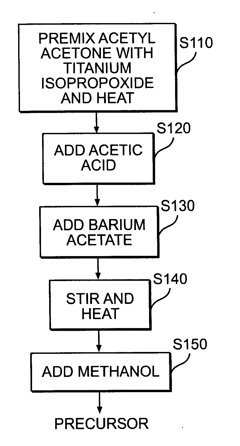
[0063] A fired-on-foil thin film undoped BaTiO3 dielectric was formed from the following precursor solution:

Barium acetate2.6gTitanium isopropoxide2.9mlAcetylacetone2.0mlAcetic acid10.0mlMethanol15ml

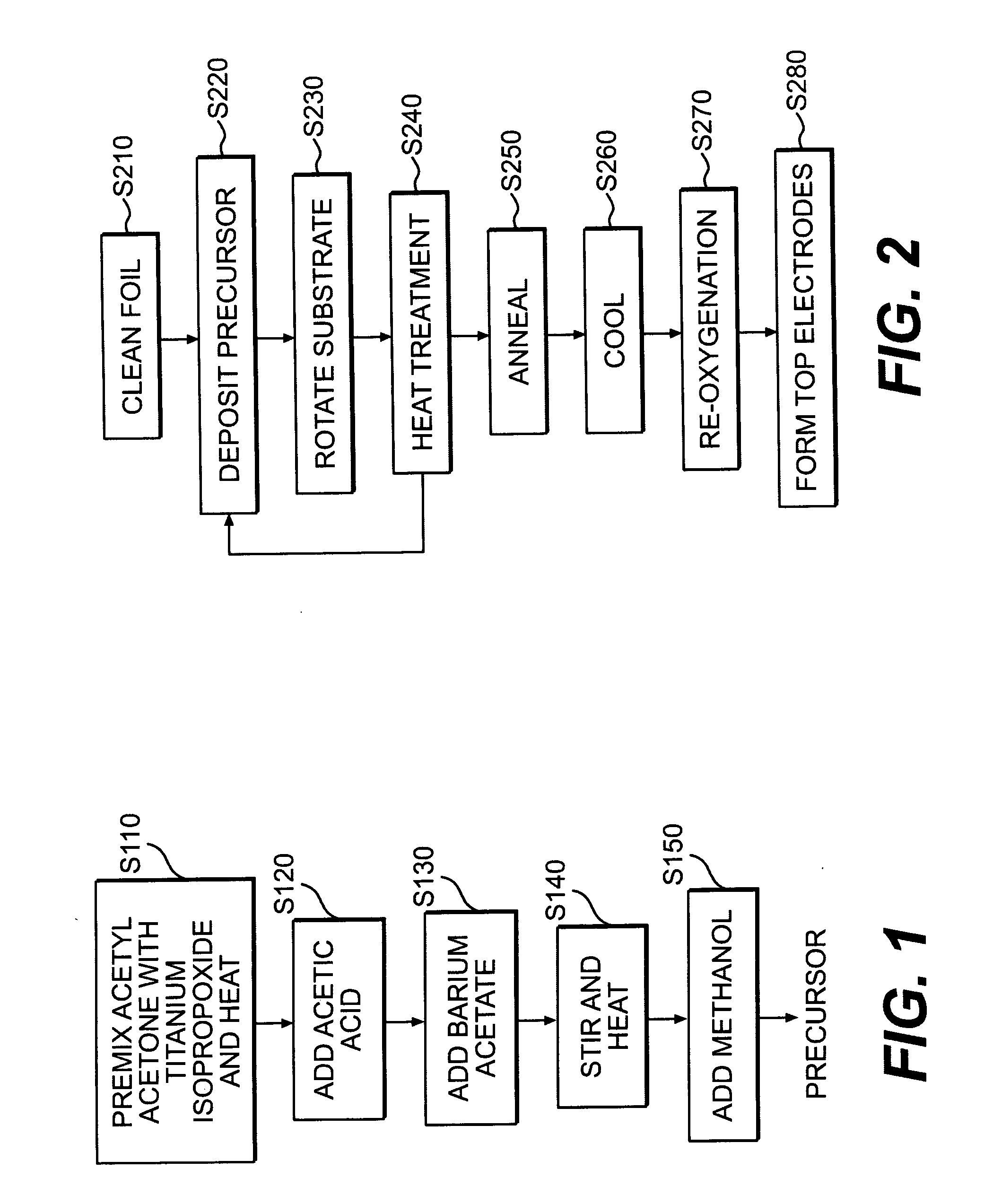
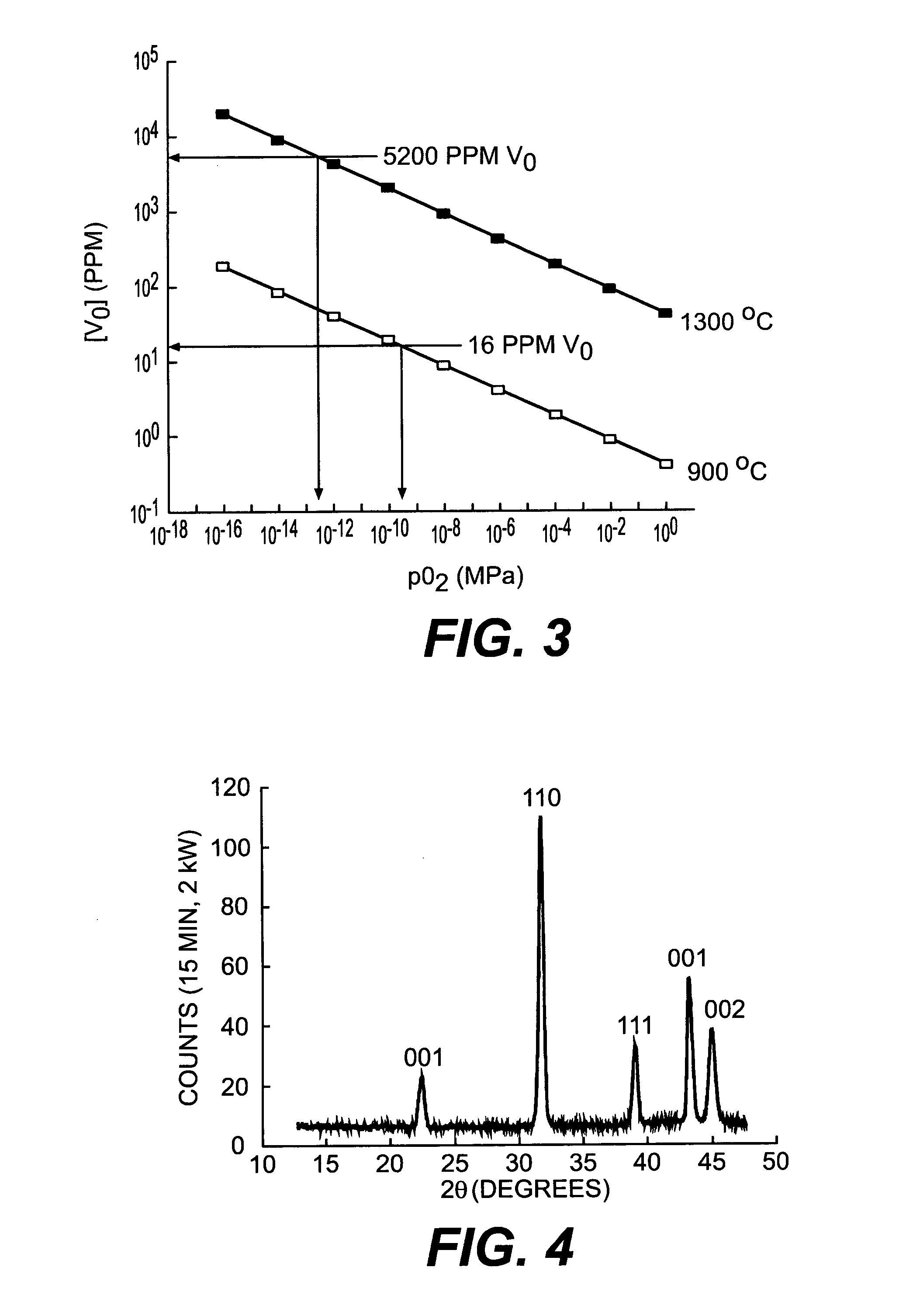
[0064] The precursor solution was prepared and deposited on a clean 0.5 oz. copper foil as described with reference to FIGS. 1 and 2. No dopants were added to the precursor solution. Annealing was performed at 900° C. for 30 minutes in an atmosphere containing a partial pressure of oxygen of 10−10 atmospheres. The annealed thickness of the resultant dielectric was approximately 0.5 micron. Re-oxygenation was performed at 600° C. for 20 minutes in an atmosphere containing a partial pressure of oxygen of 10−7 atmospheres. A top platinum (Pt) electrode was sputtered onto the dielectric.

[0065]FIGS. 4-7 show experimental data collected for the undoped BaTiO3 capacitor prepared on copper foil according to Example 1. FIG. 4...

example 2

Yttria-Doped Barium Titanate Dielectric

[0075]FIG. 9 is a plot of measured permittivity (upper data set) and loss tangent (lower data set) versus bias voltage for a thin film Y-doped BaTiO3 capacitor prepared on a copper foil substrate. Data was collected during the voltage ramp up and during the ramp down. The overlapping curves illustrate the expected hysteresis behavior. A high permittivity value of approximately 1600 was achieved with yttrium doping.

[0076] The dielectric was prepared by adding 1 mol % Y to the precursor solution as described in Example 1. The precursor was then solution-deposited to form a dielectric layer. Annealing and re-oxygenation of the dielectric layer was performed as in Example 1. The resultant dielectric composition is described generically as: (Ba1-xYx)(Ti1-yYy) O3 where 0<x<1 and 0<y<1. The specific precursor solution composition was:

Barium acetate2.6gYttrium acetate0.27gTitanium isopropoxide2.9mlAcetylacetone2.0mlAcetic acid10.0mlMethanol15ml

[007...

example 3

Barium Titanate Dielectric Prepared on Platinum Foil

[0078] In Example 3, a thin film BaTiO3 dielectric film was prepared on a platinum foil substrate, rather than a copper foil. The BaTiO3 dielectric was formed in a manner similar to that of Example 1. The x-ray line widths, from which grain size is calculable, were identical for the dielectric formed on platinum as for the BaTiO3 dielectric formed on copper foil. Accordingly, the x-ray line widths indicate average dielectric grain sizes in the range of 0.1-0.2 micron, and high crystallinity. Choice of foil material therefore appeared to have little or no effect on grain size.


PUM

PropertyMeasurementUnit
Temperatureaaaaaaaaaa

Abstract

Dielectrics are formed having high dielectric constants, low loss tangents, and other desirable electrical and physical properties. The dielectrics are annealed at temperatures allowing the use of copper foil substrates, and at low oxygen partial pressures.

Description

FIELD OF THE INVENTION [0001] The technical field is embedded capacitors. More particularly, the technical field includes capacitors having thin film dielectrics. BACKGROUND OF THE INVENTION [0002] The practice of embedding capacitors in printed wiring boards (PWB) allows for reduced circuit size and improved circuit performance. Capacitors are typically embedded in panels that are stacked and connected by interconnection circuitry, the stack of panels forming a printed wiring board. The stacked panels can be generally referred to as “innerlayer panels.” Embedded capacitors are subject to requirements such as acceptable breakdown voltage, stability of capacitance within specified temperature ranges, low dielectric loss, construction from environmentally acceptable materials, simplicity of manufacture, and amenability to printed circuit board manufacturing techniques. One industry standard, Electrical Industry Association designation X7R, requires that a capacitor's capacitance vary ...

Claims


Application Information

Patent Timeline
IPC IPC(8): H01G4/12H05K1/16H05K3/46
CPCH01G4/1218H05K1/162H05K3/4652H05K2203/125H05K2201/0355H05K2201/09509H05K2201/0175H01G4/12
Inventor BORLAND, WILLIAM J.IHLEFELD, JON FREDRICKKINGON, ANGUS IANMARIA, JON-PAUL
Owner NYTELL SOFTWARE LLC
Learn More