Surface emitting dfb laser structures for broadband communication systems and array of same

a laser structure and surface-emitting technology, applied in the field of optical signal-based telecommunication systems, lasers, can solve the problems of increased cost, difficulty in necessary techniques, and difficulty in supplying signal carrier sources, and achieve the effects of reducing costs, reducing costs, and reducing costs

Inactive Publication Date: 2005-03-10
PHOTONAMI INC
View PDF45 Cites 29 Cited by
  • Summary
  • Abstract
  • Description
  • Claims
  • Application Information

AI Technical Summary

Benefits of technology

[0013] What is needed is a surface emitting laser structure which is both suitable for telecommunications applications and which avoids the defects of the prior art. More particularly what is needed is a laser structure where the mode is controlled precisely and efficiently to permit fibre coupling and yet which can be made using conventional lithographic techniques in the semiconductor art. An object of the present invention is to provide a low-cost optical signal source that is capable of generating signals suitable for use in the optical broadband telecommunications signal range. Most preferably such a signal source would be in the form of a semiconductor laser which can be fabricated using conventional semiconductor manufacturing techniques and yet which would have higher yields than current techniques and thus can be produced at a lower cost. It is a further object of the present invention that such a signal source would have enough power, wavelength stability and precision for broadband communications applications. What is also desired is a semiconductor laser signal source having a signal output which is easily and efficiently coupled to an optical fibre. Such a device would also preferably be fabricated as an array on a single wafer-based structure and may be integrally and simultaneously formed or fabricated with adjacent structures such as signal absorbing adjoining regions and photodetector devices.

Problems solved by technology

As well, the cost of supplying signal carrier sources becomes an issue as a function of data traffic since the data density is less, the closer to edge of the network one is.
A drawback of edge emitting DFB laser signal sources is that the beam shape is in the form of a short stripe, strongly diverging in two dimensions with differing divergence angles due to the small aperture of the emitting area, which requires a spot converter to couple the signal to a single mode fibre.
The necessary techniques are difficult and can be lossy, resulting in increased cost.
Although they can achieve good performance once finished and coupled to the fibre, edge emitting DFB lasers have several fundamental characteristics that make them inefficient to produce and hence more expensive.
However, the yield of viable edge emitting DFB lasers (i.e. those which meet the desired signal output specifications) obtained from a given wafer can be low due to a number of factors in the final fabrication or packaging steps.
If symmetric coatings (usually anti-reflective) are applied to both surfaces, then the two main modes of the laser are degenerate and there no a priori discrimination between modes, leading to poor control of the SMSR and therefore poor single mode yield.
Uncertainty in the phase introduced by the cleaving step results in poor control of the lasing wavelength.
Therefore lasers produced in this way generally have poor single mode yield, wavelength yield, or both and are not optimal for use in DWDM systems.
This compounds the inefficiency of such low yields from the wafer due to multimode behaviour (poor SMSR) or incorrect wavelength.
This structure suffers from spatial hole burning as a result of the intense field generated in the region of the phase shift.
This limits the output power of the device.
Further, the laser is very sensitive to even small reflections from the facets, adding a source of instability and difficulty due to the need for high quality anti-reflection coatings on the facets.
These designs have only recently been practical due to advances in the required semiconductor fabrication techniques.
Gain and loss coupled designs still, however, require cleaving and coating of the facets before the chip can be tested.
As well, the emission is still from the edge and coupling into a fibre remains a problem.
The dual-lobed shape can only be coupled to a fibre with poor efficiency.
This method is difficult to implement due to the lithography involved and the design leads to a deterioration of other specifications related to an increase in spatial hole burning in the region of the phase shift.
Furthermore, the lower efficiency of the radiation coupling and low coupling coefficient of the index-coupled versus the gain coupled design lead to a low power from the surface as well as relatively high threshold current for the device.
Similarly, U.S. Pat. No. 4,958,357 directly introduces a phase shift in a surface emitting, index coupled, second order grating DFB laser with similar difficulties resulting.
While purporting to offer wafer-evaluation and an elimination of facet-cleaving due to surface emission, this patent teaches a complex structure which is difficult to build and even more difficult to control.
While various schemes are proposed to mitigate spatial hole burning these add complexity and in any event are not successful.
Thus, scale-up is limited by spatial hole burning.
While interesting, this patent does not disclose how the grating affects fibre coupling efficiency (since it is not concerned with any telecom applications).
This patent also fails to teach what parameters control the balance between total output power and fibre coupling efficiency or how to effectively control the mode.
Lastly, this patent fails to teach a surface emitting laser which is suitable for telecommunication wavelength ranges.
Such attempts have been unsuccessful for a number of reasons.
Such devices tend to suffer from a difficulty in fabrication due to the many layered structure required as well as a low power output due to the very short length of gain medium in the cavity.
The short cavity is also a source of higher noise and broader linewidth.
The broader linewidth limits the transmission distance of the signal from these sources due to dispersion effects in the fibre.

Method used


Image

  • Surface emitting dfb laser structures for broadband communication systems and array of same
  • Surface emitting dfb laser structures for broadband communication systems and array of same
  • Surface emitting dfb laser structures for broadband communication systems and array of same

Examples


Embodiment Construction

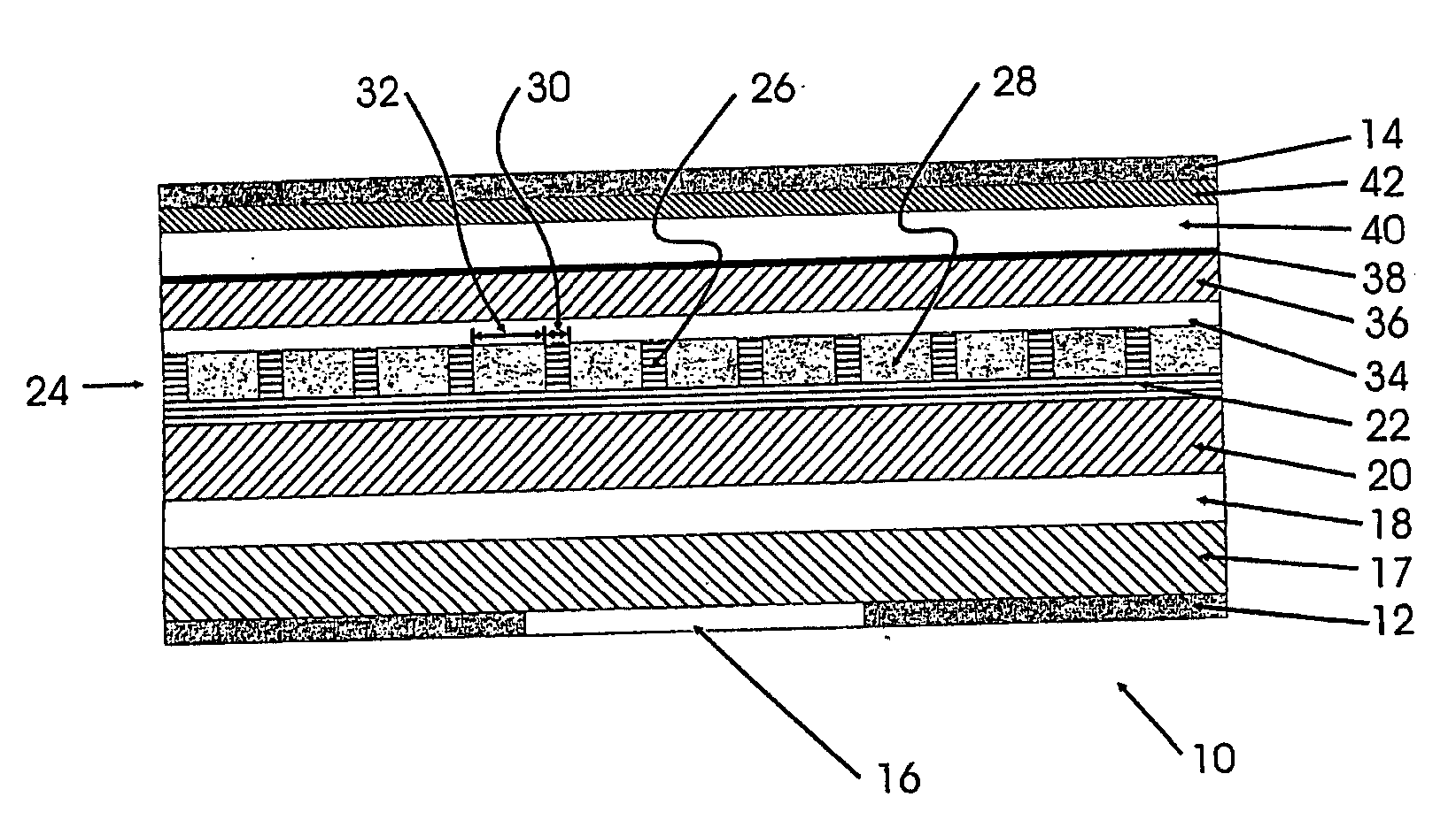
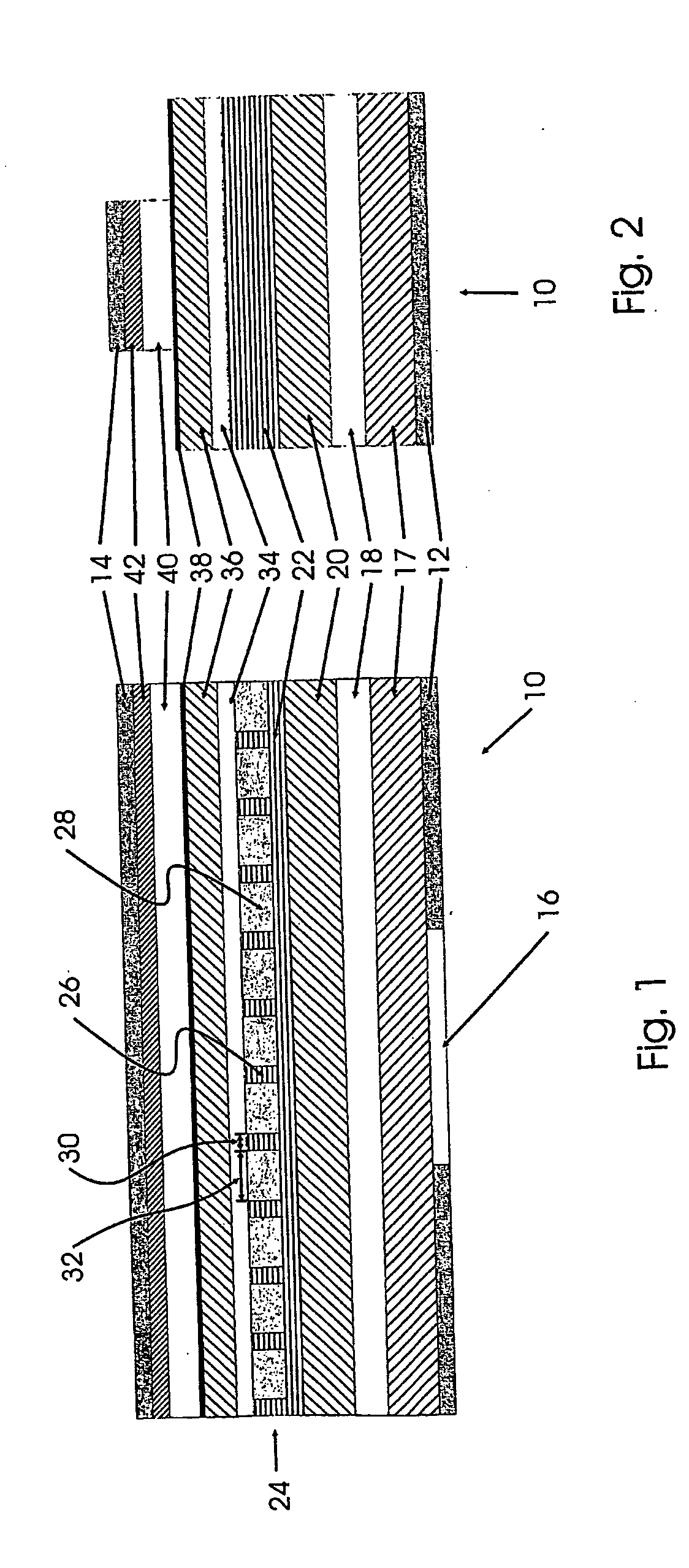
[0038]FIG. 1 is a side view of one embodiment of a surface emitting semiconductor laser structure 10 according to the present invention, while FIG. 2 is an end view of the same structure. The laser structure 10 is comprised of a number of layers built up one upon the other using, for example, standard semiconductor fabrication techniques. It will be appreciated that the use of such known semiconductor fabrication techniques for the present invention means that the present invention may be fabricated efficiently in large numbers without any new manufacturing techniques being required.

[0039] In this disclosure the following terms shall have the following meanings. A p-region of a semiconductor is a region doped with electron acceptors in which holes (vacancies in the valence band) are the dominant current carriers. An n-region is a region of a semiconductor doped so that it has an excess of electrons as current carriers. An output signal means any optical signal which is produced by ...


PUM


Abstract

A surface emitting semiconductor laser (10) is shown having a semiconductor lasing structure having an active layer (22), opposed cladding layers contiguous to said active layer, a substrate (17), and electrodes (12,14) by which current can be injected into the semiconductor lasing structure. Also included is a second or higher order distributed diffraction grating (24) having periodically alternating elements, each of the elements being characterized as being either a high gain element (26) or a low gain element (28). Each of the elements has a length, the length of the high gain element and the length of the low gain element together defining a grating period, where the grating period is in the range required to produce an optical signal in the optical telecommunications signal band. The total length of the high gain elements is no more than the total the lengths of the low gain elements. A single laser structure may be provided or an array of side by side laser structures on a common substrate is also provided. In a further aspect a method of testing laser structures on wafer is provided.

Description

FIELD OF THE INVENTION [0001] This invention relates generally to the field of telecommunications and in particular to optical signal based telecommunication systems. Most particularly, this invention relates to lasers, such as semiconductor diode lasers, for generating carrier signals for such optical telecommunication systems. BACKGROUND OF THE INVENTION [0002] Optical telecommunications systems are rapidly evolving and improving. In such systems individual optical carrier signals are generated, and then modulated to carry information. The individual signals are then multiplexed together to form dense wavelength division multiplexed (DWDM) signals. Improvements in optical technology have led to closer spacing of individual signal channels, such that it is now common for 40 signal channels to be simultaneously deployed in the C-band, with 80 or even 160 simultaneous signal channels in the combined C+L bands beginning to be deployed in the near future. [0003] Each signal channel req...

Claims


Application Information

Patent Timeline
Patent Type & Authority Applications(United States)
IPC IPC(8): H01S1/00H01S5/026H01S5/0683H01S5/12H01S5/187H01S5/40
CPCH01S5/0264H01S5/0683H01S5/12H01S5/4087H01S5/1228H01S5/187H01S5/4025H01S5/1203H01S3/08
Inventor SHAMS-ZADEH-AMIRI, ALI M
Owner PHOTONAMI INC
Why Eureka
Try Eureka