

Two step post-deposition treatment of ILD layer for a lower dielectric constant and improved mechanical properties
a dielectric layer and mechanical and insulating technology, applied in the field of semiconductor device manufacturing, can solve the problems of large increase in dielectric constant, degrade device performance, etching and polishing action, etc., and achieve the effects of improving mechanical properties, reducing dielectric constant, and improving hardness and thermal stability of composite materials
- Summary
- Abstract
- Description
- Claims
- Application Information
AI Technical Summary
Benefits of technology
Problems solved by technology
Method used
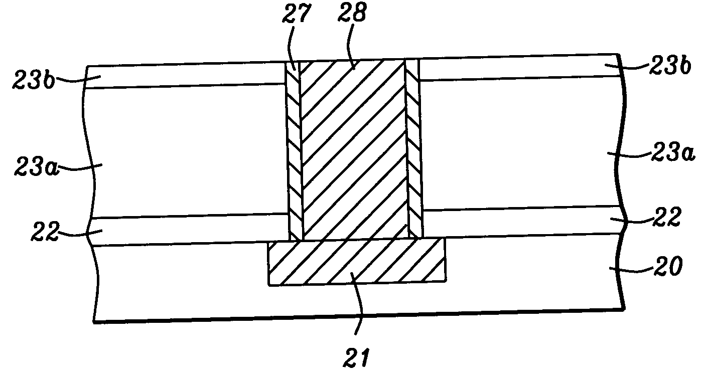
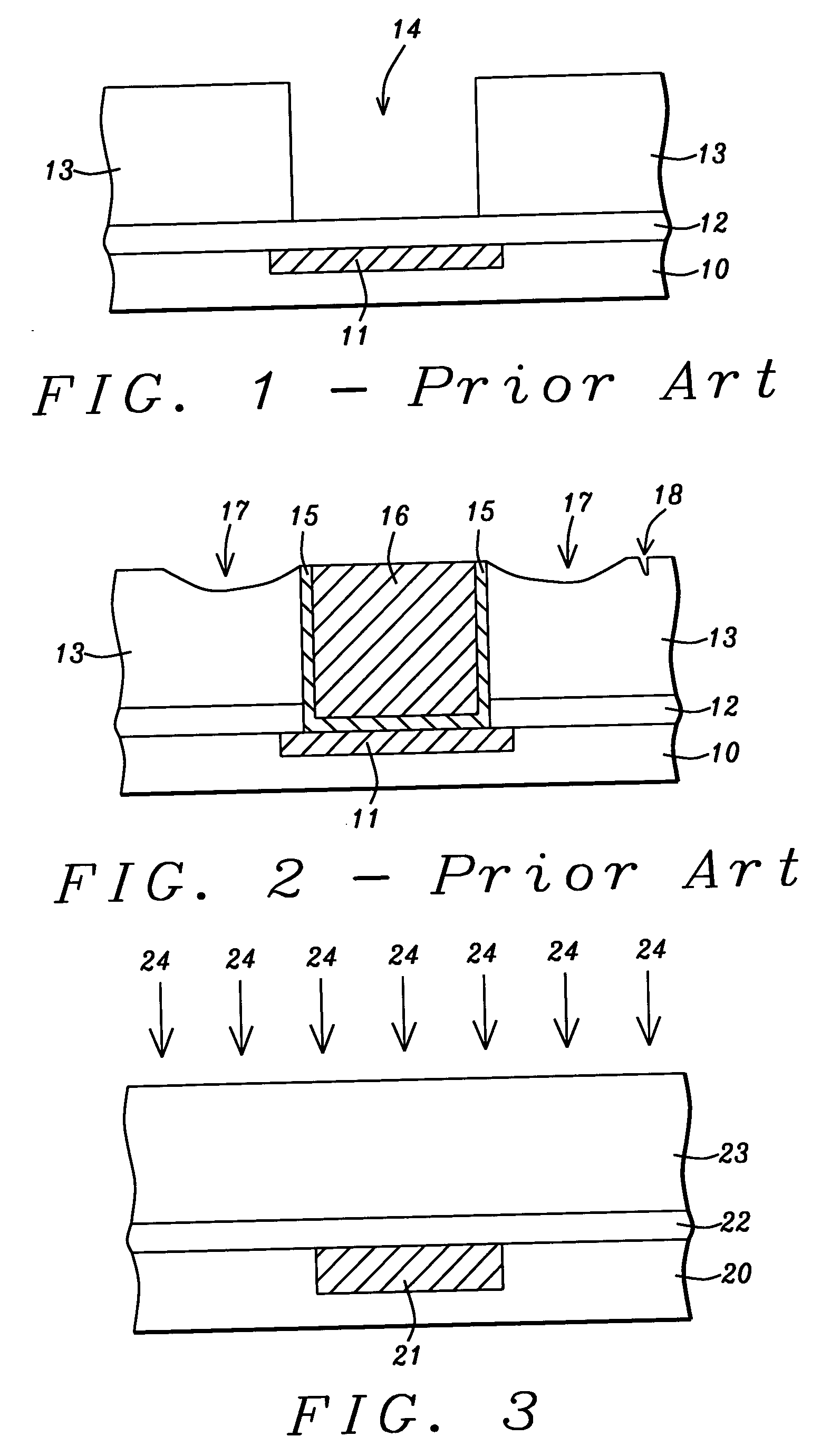
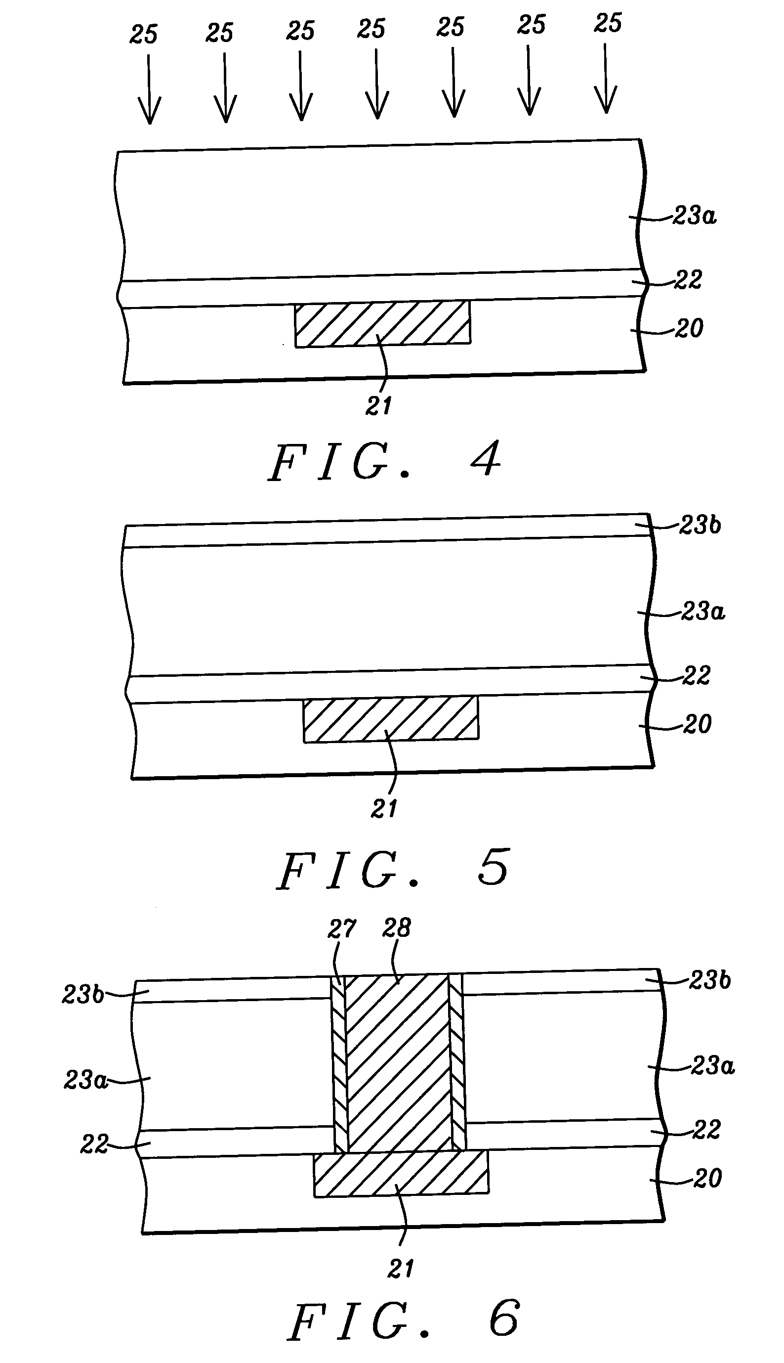
Image

Examples
example 1
[0063] This example illustrates the advantage of the present invention with regard to a further lowering of the dielectric constant in a low k dielectric layer by a post-deposition plasma treatment. A 5000 Angstrom thick SiCOH layer was deposited on several silicon wafers in a CVD process chamber using a PECVD process comprising 2,4,6,8-tetramethylcyclotetrasiloxane(TMCTS), CH4, and O2 precursors at flow rates of 6400, 1600, and 1600 sccm, respectively at 250° C. with a chamber pressure of 5 torr, and a RF power of 1000 Watts. The wafers were cured by baking at 400° C. in an oven for 60 minutes. A k value of 3.0 was observed by a measurement performed with a Hg probe as shown in Table 1. Sample 1 was obtained by subjecting a first wafer with a SiCOH layer to H2 plasma with a RF power of 900 Watts, a H2 flow rate of 1800 sccm, a chamber pressure of 5 torr, and a substrate temperature of 400° C. for 60 seconds. Sample 2 was generated in a similar fashion except that a He flow rate of ...
PUM
| Property | Measurement | Unit |
|---|---|---|
| pressure | aaaaa | aaaaa |
| pressure | aaaaa | aaaaa |
| RF power | aaaaa | aaaaa |
Abstract
Description
Claims
Application Information