Polishing method

a metal film and polishing technology, applied in lapping machines, other chemical processes, manufacturing tools, etc., can solve the problems of excessive polishing, difficult microprocessing by dry etching which was used with aluminum alloy, and difficult microprocessing by dry etching, etc., to reduce peeling, reduce scratches, and control dishing

Inactive Publication Date: 2005-04-07
RENESAS ELECTRONICS CORP
View PDF18 Cites 33 Cited by
  • Summary
  • Abstract
  • Description
  • Claims
  • Application Information

AI Technical Summary

Benefits of technology

[0039] This invention, which was conceived in view of the aforesaid problems, therefore aims to provide a polishing method and semiconductor manufacturing method which permit at least one of the following to be attained: (1) control of dishing and erosion in the formation of an

Problems solved by technology

To achieve higher speeds of LSI attempts are being made to use low resistance copper alloy instead of the conventional aluminum alloys as an interconnection material, however with copper alloy, microprocessing by dry etching which was used with aluminum alloy is difficult.
However, when interconnections and plugs were formed by CMP using a conventional slurry containing a solid abrasive for metal film polishing as a main component the following problems (1)-(8) occurred.
However, it is known that when CMP is applied to a wafer where a metal film is deposited on an insulating film having a groove which is an interconnection pattern, excessive polishing occurs locally.
This is due to the fact that there is unevenness on the surface of the metal film before CMP is performed, reflecting the groove which is the interconnection pattern.
There fore dishing and erosion become conspicuous problems in pads of large area (area of about 0.1 mm side) or with crowded interconnection patterns.
(2) Scratches (polishing marks) occur due to the solid abrasive used for polishing.
Therefore, scratches occur on the surface of an insulating film exposed by CMP in addition to the surface of the metal film used for the interconnection.
Slurry remains behind in the scratches on the insulating film surface and causes malfunction of the semiconductor device due to heavy metal ion contamination.
It also affects the shape of the upper layer interconnection, and causes short circuits.
The scratches on the metal film surface cause poor continuity and deterioration of electromigration resistance.
However, it is difficult for even this method to prevent scratches in a soft metal such as copper.
The scratches can be reduced by using a soft polishing pad, but dishing and erosion become more serious, and flatness after CMP deteriorates.
A new problem however arises in this case that-the throughput falls.
To prevent peeling, the down force and platen rotation speed may be reduced, but if it is attempted to completely prevent it, the CMP rate falls and polishing time becomes longer which is not practical.
This can be resolved by using a soft polishing pad, but dishing and erosion become serious, and flatness after CMP deteriorates.
The cleaning technique is very complicated as shown in FIG. 11.
(5) Consumable items used for CMP are costly.
This is because the production cost of abrasives used in the slurry is high, and great care must be taken to adjust particle size.
When CMP is performed, polishing abrasive adheres to this polishing pad, clogging occurs, and the CMP rate drops.
Therefore the life of the polishing pad was short and it was a high cost consumable item second to the polishing abrasive.
Therefore, the cost of the whole CMP facility became very high.
The co

Method used


Image

  • Polishing method
  • Polishing method
  • Polishing method

Examples


embodiment 1

[0122] A method of forming a copper interconnection by performing CMP on according to this embodiment will be described.

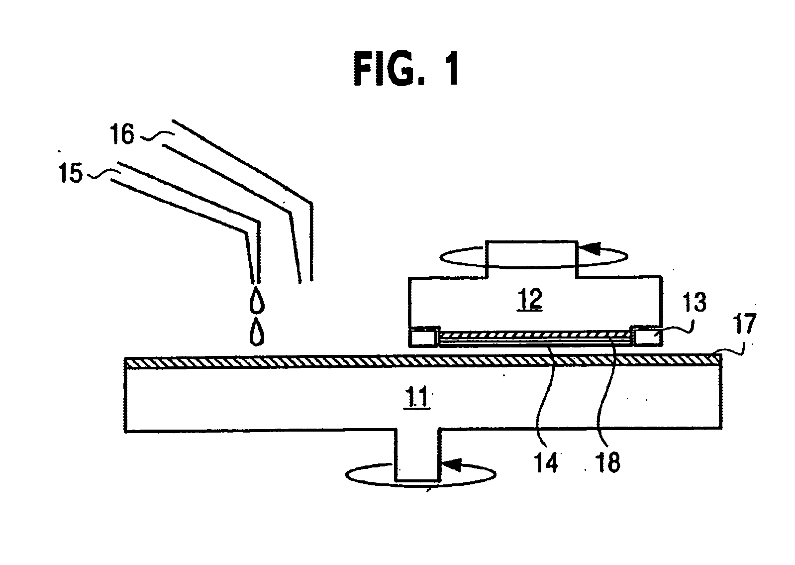
[0123]FIG. 1 is a schematic view showing a CMP machine used in this embodiment of the invention.

[0124] To perform CMP, a holder 12 which supports a wafer 14 by a backing pad 18 is rotated on a platen 11 to which a polishing pad 17 is attached A retainer ring 13 is provided so that the wafer does not come off during CMP. The down force in CMP was 220 g / cm2, and the rotation speed of platen and holder was 60 rpm. However, the down force and rotation speed are not limited to this.

[0125] In general, the CMP rate is faster if the load and rotation speed are increased, but scratches occur more easily as shown in FIG. 25. However, as the polishing abrasive concentration is low or zero in this invention, not many scratches occur relative to the load The polishing pad used was the polishing pad IC1000 manufactured by the Rodel company.

[0126] The polishing solution of th...

embodiment 2

[0144] In this embodiment, a method will be described where an inhibitor is added to the polishing solution used in Embodiment 1 to further improve polishing characteristics.

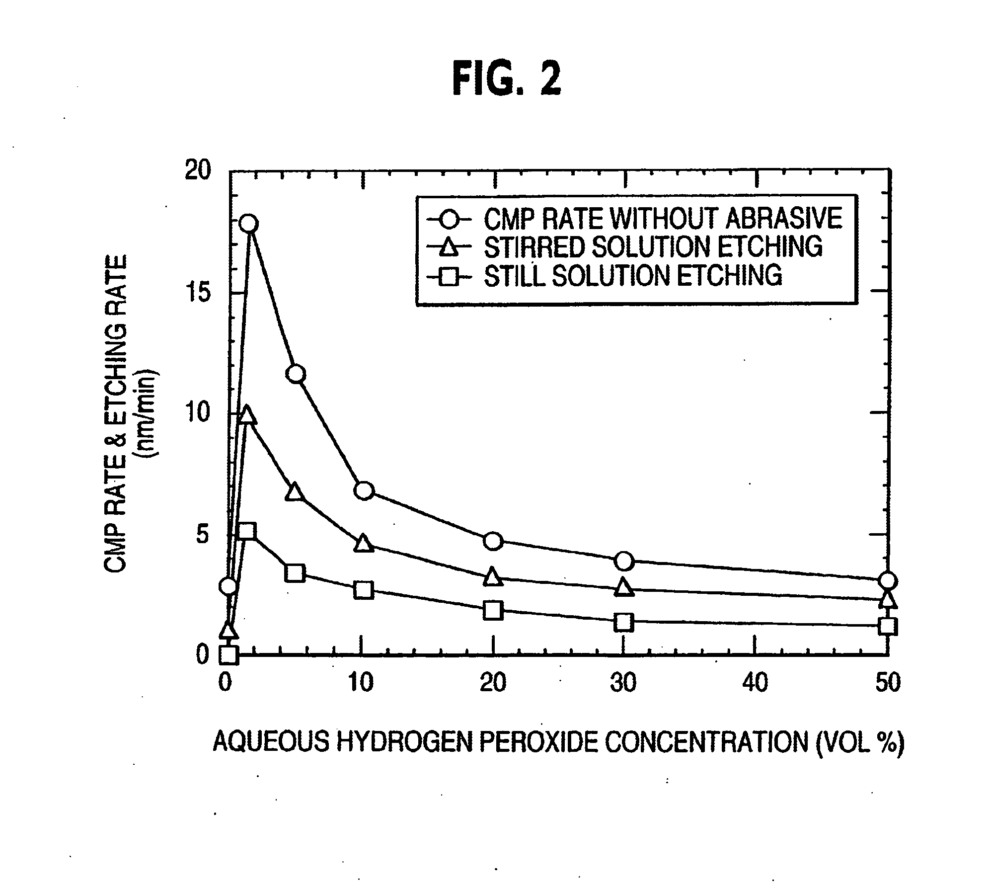
[0145] Due to the addition of the inhibitor, the etching rate shown in FIG. 3 decreases, and the ratio of CMP rate to etching rate further increases. As a result, excessive etching of the copper surface during CMP can be prevented and oxidation of the polished copper surface after CMP can be prevented.

[0146] The inhibitor was BTA. 0.1 wt % BTA was added to a polishing solution comprising 5 vol % aqueous hydrogen peroxide and 0.03 wt % citric acid mixed with pure water.

[0147] Even when BTA is added the pH and oxidation-reduction potential of the polishing solution hardly change, and remain in the domain of corrosion of copper shown in FIG. 9.

[0148] The etching rate was measured as in Embodiment 1, and was found to have decreased to about ⅙ compared with the solution before BTA was added.

[0149] CMP was perfor...

embodiment 3

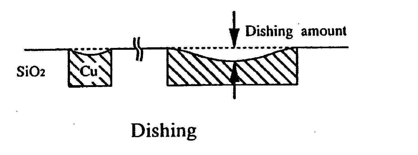
[0154] In this embodiment, the suppression of dishing and erosion due to decrease of the abrasive concentration was examined. The polishing solution of Embodiment 2 (5 vol % aqueous hydrogen peroxide, 0.03 wt % citric acid and 0.01 % BTA mixed with pure water), and the same polishing solution with 2.5 wt % added alumina abrasive (particle diameter: approx. 200 nm) as a comparison were prepared.

[0155] An inlaid interconnection was formed as in Embodiment 2 using these polishing solutions, and the line width dependence of dishing and erosion defined in FIGS. 5A-5B was measured for a width of 0.4-90 μm by photographing a 400 μm length of the interconnection in section with a scanning electron microscope (SEM).

[0156]FIGS. 6A, 6B show the measurement results, and FIGS. 7A, 78, 8A, and 8B show sections which were drawn based on the SEM observations.

[0157] From FIGS. 6A, 6B it is seen that the dishing amount and erosion amount increased as the line width increased. However, the dishing ...


PUM

PropertyMeasurementUnit
Speedaaaaaaaaaa
Concentrationaaaaaaaaaa
Solubility (mass)aaaaaaaaaa

Abstract

A polishing technique wherein scratches, peeling, dishing and erosion are suppressed, a complex cleaning process and slurry supply/processing equipment are not required, and the cost of consumable items such as slurries and polishing pads is reduced A metal film formed on an insulating film comprising a groove is polished with a polishing solution containing an oxidizer and a substance which renders oxides water-soluble, but not containing a polishing abrasive.

Description

BACKGROUND OF THE INVENTION [0001] 1. Field of the Invention [0002] This invention relates to polishing of a metal film, and in particular to a method of polishing a metal film in a semiconductor device interconnection process. [0003] 2. Description of Related Art [0004] In recent years, as semiconductor integrated circuits (referred to hereafter as LSI) become more complex, new microtechniques are being developed. One of these is chemical mechanical polishing (referred to hereafter as CMP), which is often used in LSI manufacture in particular flattening of interlayer insulating films, forming metal plugs and inlay of interconnections in multi-layer interconnection processes. [0005] This technology is disclosed, for example, in U.S. Pat. No. 4,944,836. [0006] To achieve higher speeds of LSI attempts are being made to use low resistance copper alloy instead of the conventional aluminum alloys as an interconnection material, however with copper alloy, microprocessing by dry etching wh...

Claims


Application Information

Patent Timeline
IPC IPC(8): B24B37/00B24B37/04C09G1/02C09K3/14H01L21/02H01L21/304H01L21/321
CPCB24B37/04C09G1/02C09K3/1463H01L21/7684H01L21/02074H01L21/3212C23F3/06H01L21/302
Inventor KONDO, SEIICHIHOMMA, YOSHIOSAKUMA, NORIYUKITAKEDA, KENICHIHINODE, KENJI
Owner RENESAS ELECTRONICS CORP
Why Eureka
Try Eureka