
Forming a passivating aluminum fluoride layer and removing same for use in semiconductor manufacture

Inactive Publication Date: 2006-01-05
EKC TECH
View PDF23 Cites 20 Cited by
  • Summary
  • Abstract
  • Description
  • Claims
  • Application Information

AI Technical Summary

Benefits of technology

[0031] The novel cleaning compositions of the invention can exhibit synergistically enhanced cleaning action and cleaning capabilities at low temperatures that are generally not possible from the use of the individual components, or the components in combination with other cleaning components, such as ethoxyethanolamine or alkylamides.
[0032] It is a general object of the invention to provide a semiconductor substrate cleaning composition that is effective at low temperatures.
[0035] It is a further object of the invention to provide such a cleaning solution having low etch rates of silicon oxide.
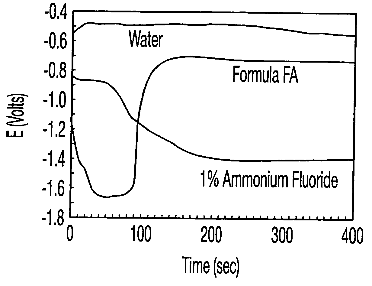
[0040] It is a further object of the invention to provide a composition which removes a fluorinated aluminum surface from an aluminum-containing layer of a substrate.
[0044] A process for cleaning residue from a substrate in accordance with this invention can include contacting the substrate with an organoammonium and amine carboxylate free composition containing one or more fluoride compounds, water and an organic amide solvent at a temperature and for a time sufficient to clean the substrate. Advantageously, the composition can have a very low corrosion rate on silica (i.e., less than about 5 Å / min, preferably less than about 2 Å / min), and optionally a low corrosion rate on, e.g., TEOS and / or BPSG.

Problems solved by technology

The substrate is often contaminated from previous process steps with monolayer amounts of metal, anions and / or organic contaminants or surface residues (particles).
Unless the cleaning conditions are carefully monitored (time, temperature, solution composition) the substrates can be damaged, as reported by Rafols, C. et al., J.
The fluoride chemistries can be very aggressive and can result in isotropic etching (etching equally in all directions).
A disadvantage of forming this protective sidewall deposit is that it can be very difficult to remove the residue after the etching procedure.
If the components in these residues are not removed or neutralized in some manner then the residues will absorb moisture and form acidic species that can corrode the metal structures.
The resultant acid corrodes wiring materials to bring about an adverse effect such as an increase in electrical resistance and wire disconnection.
Such problems frequently occur, in particular in aluminum and aluminum alloys generally used as wiring material.
The wafer substrate in contact with acidic materials, if not controlled, can destroy the metal structures.
Cleaning compositions used for removing photoresist coatings if not already ashed and other substrates have for the most part been highly flammable, generally hazardous to both humans and the environment, and comprise reactive solvent mixtures exhibiting an undesirable degree of toxicity.
Moreover, these cleaning compositions are not only toxic, but their disposal is costly since they might have to be disposed of as a hazardous waste.
In addition, these compositions generally have severely limited bath life and, for the most part, are not recyclable or reusable.
Contact holes opened on to the TiSi2 have also been difficult to clean with HF solutions since there appears to be an attack of the underlying TiSi2 layer.
There may also be difficulty with mass transport of the chemicals in the narrow hydrophilic contact holes, as taught by Baklanov, M. R. et al., Proc. Electrochem. Soc., 1998, 97-35, pp.
In many cases, the components of the cleaning compositions are relatively toxic reactive solvent mixtures and thus must be subject to stringent use conditions and require hazardous chemical handling procedures and wearing of safety garments and apparel by users so as to avoid contact with the cleaning compositions.
Additionally, because many of the toxic components of such cleaning compositions are highly volatile and subject to high evaporation rates, they require special human and environmental safety precautions to be taken during storage and use of the compositions.
This means that compositions that were suitable for cleaning less sophisticated integrated circuit substrates may not be able to produce satisfactory results with substrates containing more advanced integrated circuits in the process of fabrication.

Method used


Image

  • Forming a passivating aluminum fluoride layer and removing same for use in semiconductor manufacture
  • Forming a passivating aluminum fluoride layer and removing same for use in semiconductor manufacture
  • Forming a passivating aluminum fluoride layer and removing same for use in semiconductor manufacture

Examples


example 1

[0117] A group of cleaning chemistries containing the ingredients of ammonium fluoride, water, one or more amides, such as N,N-dimethylacetamide, N,N-dimethylformamide, 1-methyl-2-pyrrolidinone, N,N-dimethylpropionamide, and dimethyl sulfoxide listed in Table 1 were tested with metal wafers having stacks of TEOS / Ti / TiN / AICu / TiN (from Bottom to Top), etched with Cl2 / BCl3 plasma in a commercially available AMT DPS etcher. The resulting metal wafers with residues were cut into small sample pieces, and then the sample pieces were immersed into the chemistry solutions in Table 9 for cleaning for 5 minutes at room temperature. The sample pieces were taken out, rinsed with deionized water, and dried with a flow of N2. SEM was performed with a Hitachi 4500 FE-SEM for evaluating cleaning and corrosion effects. Residue removal and corrosion effects on metal stack were assessed by visual comparisons and were all ranked on a scale of 1 to 10. The formulations in Table 9 are shown in weight perc...

example 2

[0119] Based on the results in Example 1, N,N-dimethylacetamide and dimethyl sulfoxide were chosen to optimize the cleaning formulations with ammonium fluoride and water. A commercially available LAM TCP9600 etcher with a Cl2 / BCl3 plasma was used for etching metal wafers with a stack of Oxide / Ti / TiN / AlCu / TiN (from bottom to top). The resulting metal wafers with residues were cut into small sample pieces, and the sample pieces were immersed into the cleaning solutions in Table 10 for cleaning for 5 minutes at room temperature. The sample pieces were taken out, rinsed with deionized water, and dried with a flow of N2. SEM was performed with a Hitachi 4500 FE-SEM for evaluating cleaning and corrosion effects. Residue removal and corrosion effects on the metal stack were assessed by visual comparisons and were all ranked on a scale of 1 to 10. pH values, as reported in FIG. 3, were measured with an Orion SA520 meter with glass pH electrode. The formulations in Table 10 are shown in weig...

example 3

[0121] One of the compositions (composition N) from Table 10 was chosen to process metal wafers etched with an AMT DPS etcher with Cl2 / BCl3 plasma. After the dry etching process, heavy residues were formed on these metal wafers, as shown in the representative sample of FIG. 4. The metal wafers with the residues were cut into small sample pieces, and the sample pieces were immersed into the chosen chemistry solution for removing the heavy residues for 3, 5 and 10 minutes at room temperature. Composition N could clean the residues completely at 5 minutes and beyond but could not clean the residues completely at 3 minutes (FIGS. 5A-5C). The sample pieces were then taken out, rinsed with deionized water, and dried with a flow of N2. SEM was performed with a Hitachi 4500 FE-SEM for evaluating cleaning and corrosion effects.

[0122] Photo-removal and residue-removal technology will further evolve to meet the needs of 300 mm wafer processing. The SEZ tool and other new types of equipment ar...


PUM

PropertyMeasurementUnit
Fractionaaaaaaaaaa
Fractionaaaaaaaaaa
Fractionaaaaaaaaaa

Abstract

A composition for the cleaning of residues from substrates can contain from about 0.01 percent by weight to about 5 percent by weight of one or more fluoride compounds, from about 20 percent by weight to about 50 percent by weight water, from about 20 percent by weight to about 80 percent by weight of an organic amide solvent and from 0 to about 50 weight percent of an organic sulfoxide solvent. The composition can have a pH between about 7 and about 10, alternately from greater than 8 to about 10. Additionally, the composition optionally can contain corrosion inhibitors, chelating agents, surfactants, acids, and / or bases. In use of the composition, a substrate can advantageously be contacted with the composition for a time and at a temperature that permits cleaning of the substrate.

Description

FIELD OF THE INVENTION [0001] This invention relates to a process using semiaqueous cleaning composition that is particularly useful for cleaning organic and inorganic compounds or “polymers” (post etch residues) from a semiconductor substrate. As used herein, the term “semiaqueous” refers to a mixture of water and organic solvent. The invention also includes compositions used to treat and to clean residues from semiconductor substrates. The solutions contain fluoride compounds, water, and solvent and optionally contain corrosion inhibitors, chelating agents, surfactants, acids and bases. BACKGROUND OF THE INVENTION [0002] Fluoride containing chemistries have been used for many years to clean prime silicon wafers (wafers that have not yet undergone ion implantation or device construction) in the semiconductor industry. Normally, the fluoride chemistry (usually dilute hydrofluoric acid) is used as the last process step in the sequence called “RCA rinses”. The substrate is often conta...

Claims


Application Information

Patent Timeline
IPC IPC(8): C03C23/00
CPCC03C15/00C03C2218/33C11D7/10C11D7/3209H01L21/02071C11D7/34C11D11/0047H01L21/02063C11D7/3218C11D2111/22
Inventor CARTER, MELVIN K.
Owner EKC TECH
Learn More