[0005] This invention represents a departure from traditional detectors of the Focal Plane Array (FPA) design by employing an approach wherein the coordinate sensitivity of a microfabricated superconducting strip is controlled by scanning a beam of energy, such as from a
laser or an LCD or in the form of a
magnetic field, over the superconducting detector strip so as to physically displace the sensitive area of the detector to permit imaging over a broad spectral range. The superconducting detector strip may either be linear or curvilinear, with the latter equivalent to a
two dimensional detector array. In addition to the simplicity of the detector fabrication sequence (one step
mask transfer), a clear
advantage of this invention is the simplicity of the read-out process: an image is formed by registering the
signal with only two electrical terminals. The inventive approach can be extended for imaging over a wide spectral range; the
limiting factor being the
wavelength-dependent efficiency of thermal conversion in the film / substrate
system.
[0007] It is another object of the present invention to provide a method and apparatus for detection and imaging of
thermal radiation over a broad
wavelength range, i.e., 1 μm-1000 μm, which is commercially feasible and of relatively low cost.
[0008] A further object of the present invention is to control the coordinate sensitivity in a superconducting
microbolometer by the application of localized light or
magnetic field energy to the detector, or by the use of lithographically defined arrays of micro-heaters in the detector, to simplify the read-out mechanism.
[0010] The present invention is a method of controlling the sensitivity of specific coordinates of a low or
high temperature superconducting sensor which provides an IR sensor with broad spectral range sensitivity at relatively low cost. This method can also be applied to control the sensitivity of microbolometers made of other materials that demonstrate sharp dependence of their electrical resistance on temperature or other factors such as magnetic field, etc. Superconducting (SC) films have already been used for various x-
ray,
infrared, THz,
millimeter and
microwave applications. Superconducting
transition edge sensors have been used as calorimeters and thermistors. The unique property of SC materials is the possibility of utilizing the superconducting, resistive and magnetically ordered phases in the same substance. The type of phases depends on the fabrication methods, and on external effects. SC materials show best performance (with respect to thermal effects) for detection purposes when operating at the critical temperature (Tc), the temperature at which the material becomes superconducting. In this region, even small variations in temperature lead to substantial changes in electrical resistance.
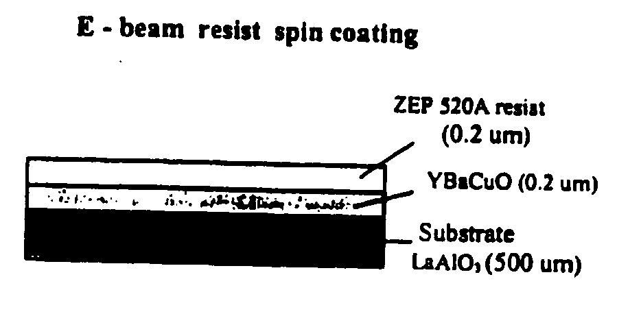
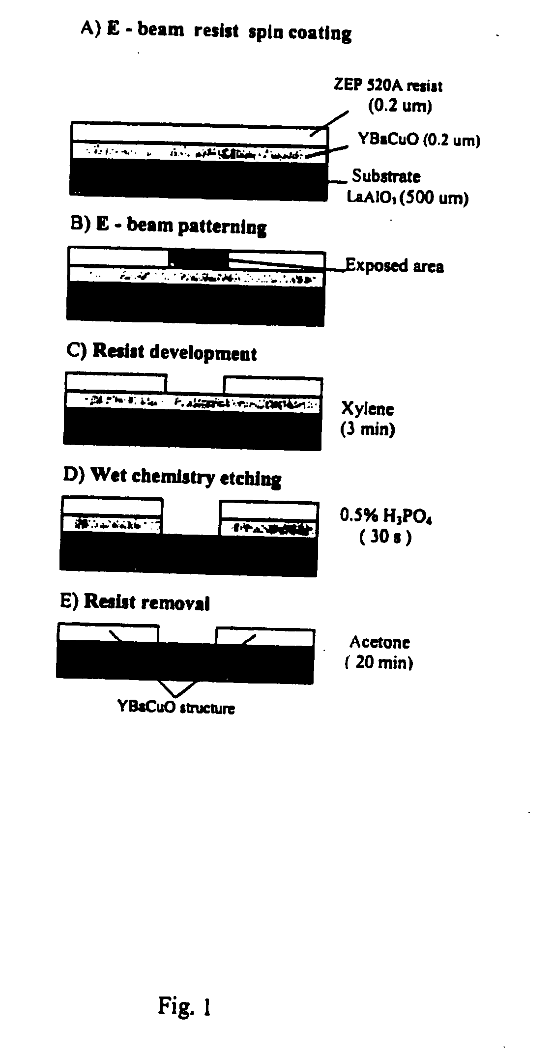
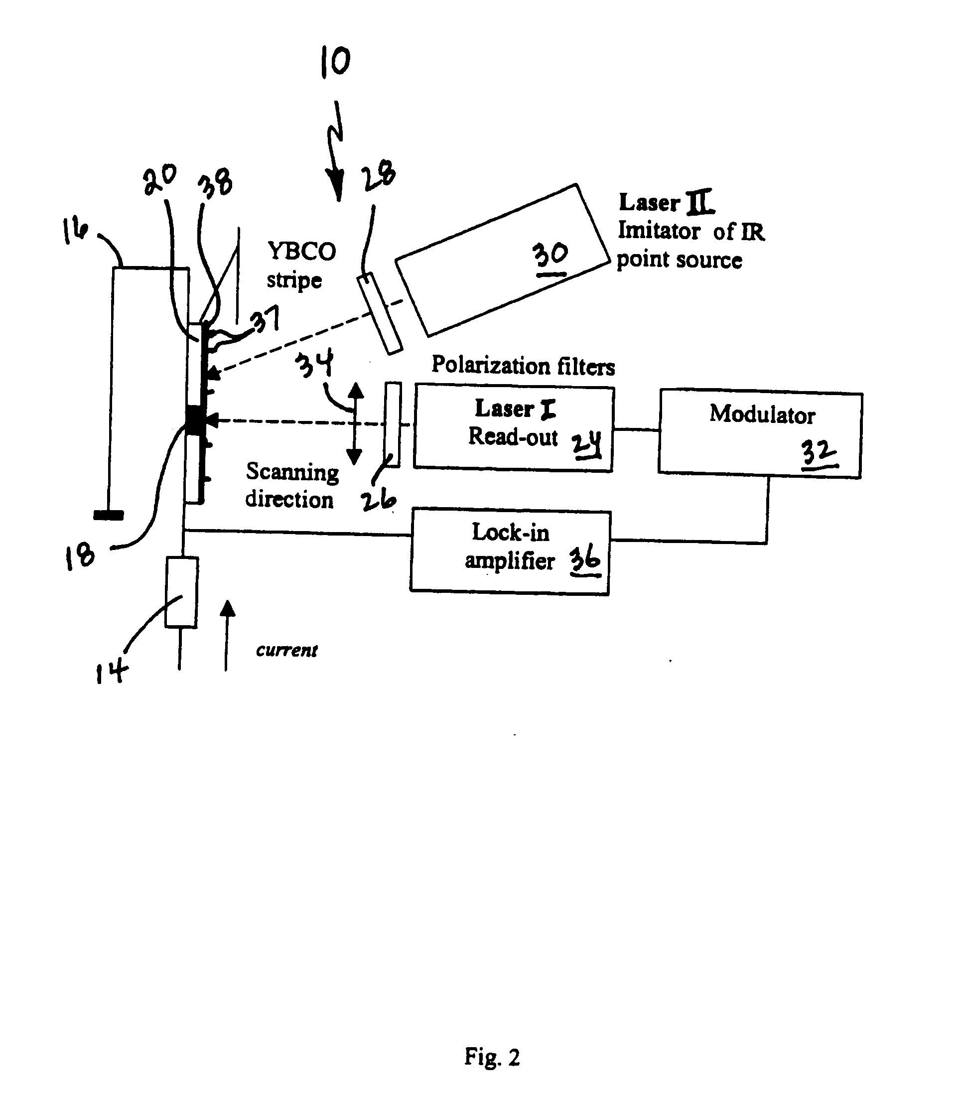
[0011] As an example, we explain the principle of this invention for the case of detection of
infrared radiation. However, this same approach can be used for imaging over a broad spectral range (from x-
ray to
millimeter wavelength). The present invention employs the external action of an optical probe, thermal heating or magnetic field to create normal, superconducting or resistive areas and control their location on the film surface. In other words, once the temperature of the SC film reaches Tc, small changes in the temperature of the film will create large measurable changes in the resistance of the film. Therefore, the invention consists of a superconducting film which may be in the form of a linear or curvilinear strip or a raster-type structure. The image to be detected is optically focused on the surface of the film. The effect of the infrared
radiation varies along the strip according to the
spatial distribution of the heat source. A laser beam, precisely focused on the SC film is used as an
external source of heat to optimally bias the sensor. By adjusting the energy of the laser, the temperature of a specific coordinate on the film can be increased up to Tc to create a local area with optimal response. The laser beam is passed over the film in a raster-like pattern which, when precisely matched with a change in resistance of the film, provides the IR temperature of the image focused on the SC film. Displacement of this resistive (and sensitive to IR
radiation) spot along the raster may be used as a basis for a self-scanning
image system. Replacement of the strip with a continuous film or curvilinear structure makes two-dimensional imaging possible. In this case, the SC film can include normal, superconducting and transition regions. However, the photo response maximum caused by thermal effects is realized in the transition region. Alternatively, a magnetic field or lithographically defined arrays of micro-heaters or a matrix of light sources (
assembly of light emitting diodes, for example) may be used in place of the laser to provide localized, pin-point heating of the SC film. The external action effect can be intensity modulated to increase the
signal-to-
noise ratio.
[0012] A subtraction of the background contribution (taken with a closed
shutter) from IR-produced images can be performed to eliminate any influence of possible sensor defects or surface temperature variation.

