

Composition and method
a porous dielectric material and composition technology, applied in the field of porous materials, can solve the problems of affecting the affecting the subsequent performance of electronic devices, and etching of porous dielectric materials with sidewall roughness,
- Summary
- Abstract
- Description
- Claims
- Application Information
AI Technical Summary
Benefits of technology
Problems solved by technology
Method used
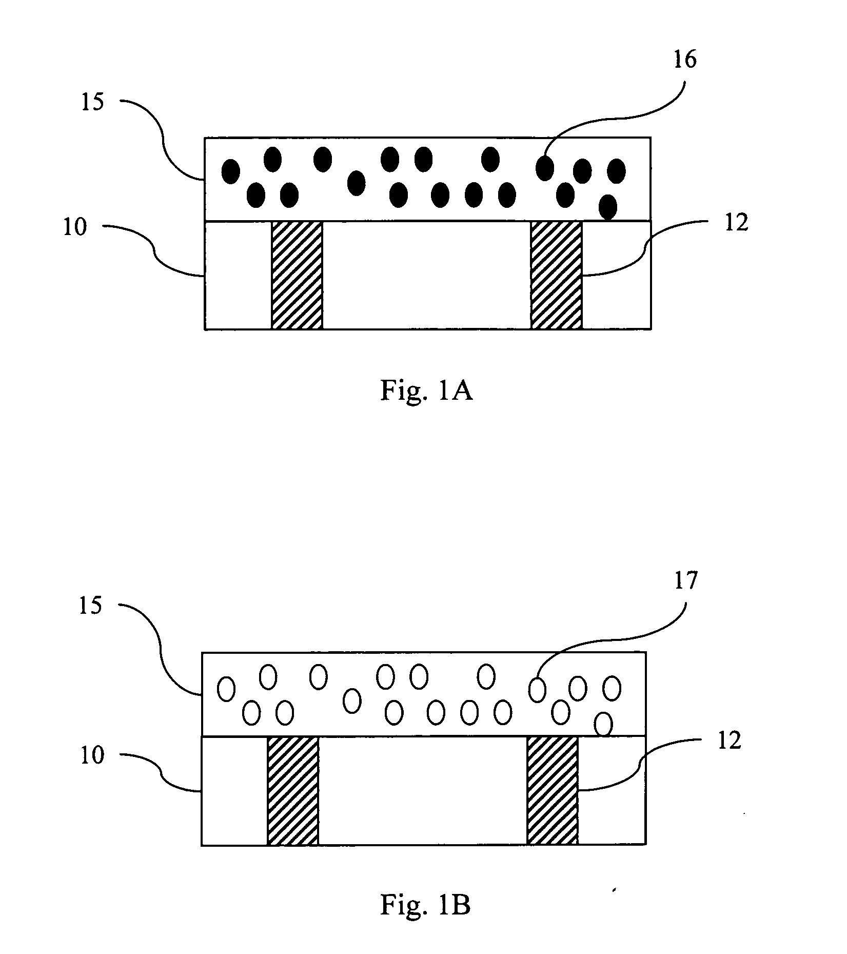
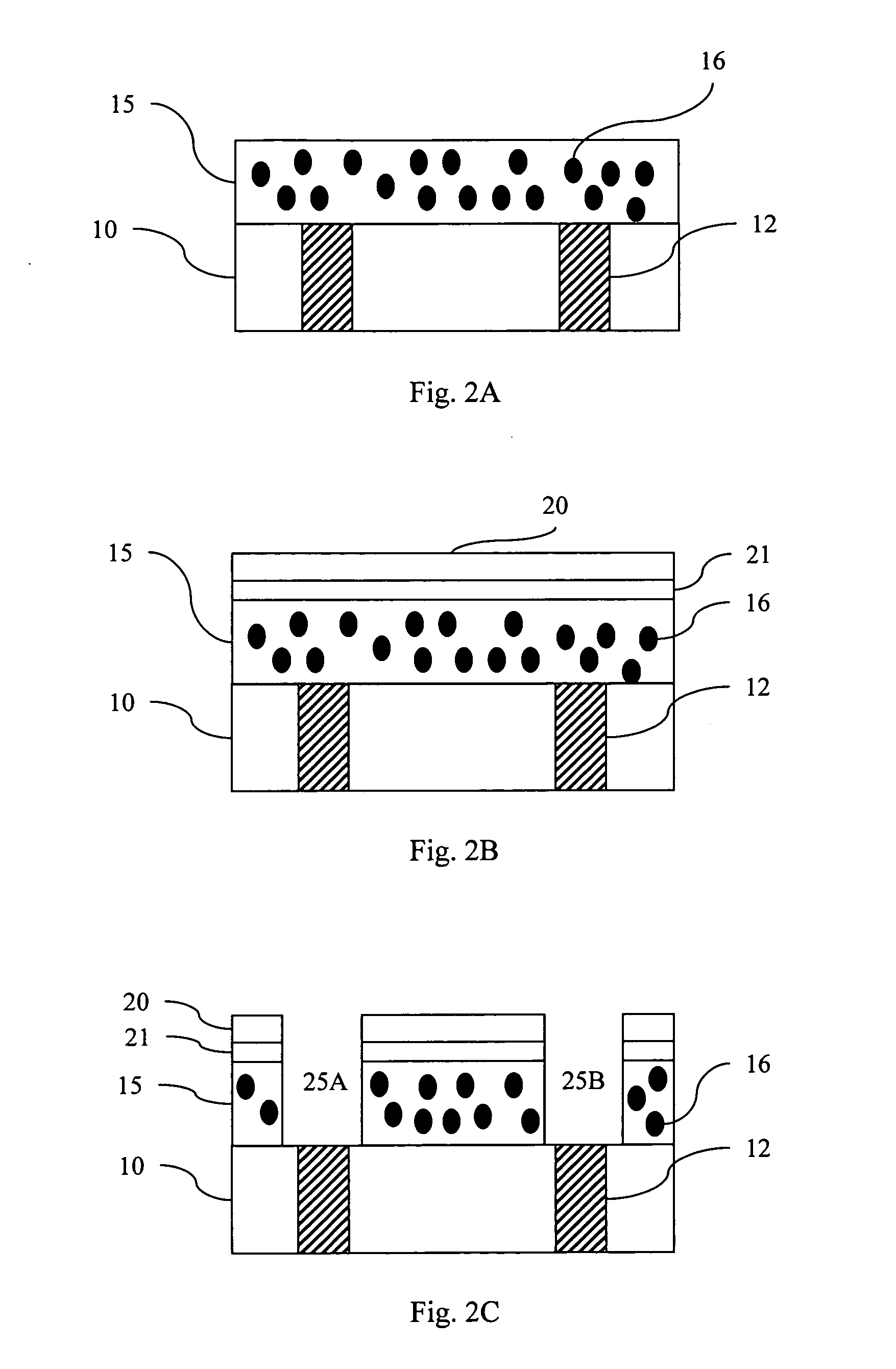
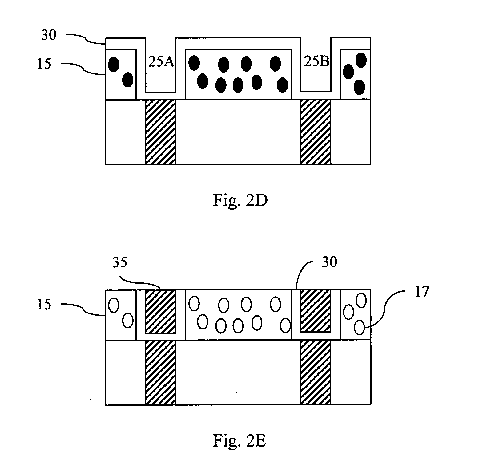
Image

Examples
example 1
[0084] A thermally removable porogen polymer particle including as polymerized units the following monomers phenoxy capped polyethylene oxide acrylate / styrene / trimthylolpropane triacrylate (in an 80 / 15 / 5 ratio by weight) was formed via solution polymerization.
[0085] A 1,000 mL reactor was fitted with a thermocouple, a temperature controller, a purge gas inlet, a water-cooled reflux condenser with purge gas outlet, a stirrer, and an addition funnel. To the addition funnel was charged 133.35 g of a monomer mixture consisting of 84.00 g phenoxy capped polyethylene oxide acrylate containing 4 moles of ethylene oxide (Mn=324, 100% purity), 15.75 g styrene (100% purity), 5.25 g trimethylolpropane triacrylate (100% purity), 2.10 g of a 75% solution of t-amyl peroxypivalate in mineral spirits (TRIGONOX 125-C75), and 26.25 g propylene glycol methyl ether acetate (“PGMEA”). The reactor, containing 544.60 g PGMEA was then flushed with nitrogen for 60 minutes while applying heat to bring the c...
example 2
[0086] The procedure of Example 1 was repeated to prepare the porogen polymers in Table 1 in the amounts specified.
TABLE 1PhOPEOAHEMAMMAStyrenePAO ChainSample(wt %)(wt %)(wt %)(wt %)TMPTALength2A80.0——15.05.042B65.07.57.515.05.042C80.0———20.042D42.515.015.015.012.542E50.015.015.07.512.542F80.00.00.07.512.542G35.015.015.015.020.042H75.0—0.010.015.042I80.07.57.50.05.042J80.03.83.87.55.042K50.015.015.015.05.042L80.02.52.55.010.042M42.515.015.07.520.042N57.515.015.0—12.542O80.03.83.8—12.542P50.015.015.0—20.042Q57.57.57.57.520.042R65.07.57.5—20.042S57.515.015.07.55.042T68.89.49.4—12.542U57.57.57.515.012.542W63.18.48.47.512.542X72.5——7.520.042Y72.5——15.012.542Z50.07.57.515.020.042AA65.0——15.020.042BB65.015.015.0—5.042CC72.511.311.3—5.042DD68.89.49.47.55.042EE80.010.0——10.042FF50.015.015.07.512.542GG50.015.015.07.512.532HH53.022.522.5—2.032II50.515.215.212.46.742JJ50.015.015.07.512.542KK80.0———20.04
[0087] In Table 1, the following abbreviations are used: PhOPEOA=phenoxy capped polyethyle...
example 3
[0088] Porous dielectric films were prepared by spin coating a composition containing porogens from Examples 1 or 2, a B-staged organic polysilica dielectric material containing 55 wt % methyl triethoxy silane (“MeTEOS”) and 45 wt % tetraethyl ortho silicate (“TEOS”) and PGMEA to a thickness of approximately 6000 to 8000 Å on a wafer. The wafers were then processed at 150° C. for 1 minute to remove solvent. The wafers were then heated to 300° on a hot plate for 3 minutes in a nitrogen atmosphere having approximately 60 ppm of O2, to cure the dielectric film. Following curing of the film, the porogens were removed by heating the samples in a furnace. The oxygen content of the furnace was below 5 ppm before heating of the sample. The sample was placed in the furnace and heated at a rate of 10° C. per minute to a temperature of 450° C. and held at this temperature for 1 hour, after which the furnace was cooled at a rate of approximately 10° C. per minute.
PUM
| Property | Measurement | Unit |
|---|---|---|
| Fraction | aaaaa | aaaaa |
| Fraction | aaaaa | aaaaa |
| Dielectric polarization enthalpy | aaaaa | aaaaa |
Abstract
Description
Claims
Application Information