Oxygen doping method to gallium nitride single crystal substrate and oxygen-doped n-type gallium nitride freestanding single crystal substrate

a gallium nitride and oxygen doping technology, which is applied in the direction of crystal growth process, polycrystalline material growth, after-treatment details, etc., can solve the problem that the device-carrying sapphire wafer cannot be divided by natural cleavage like silicon wafers, and the non-c-plane growing gan crystals cannot be made at all, so as to achieve the effect of low oxygen doping efficiency, high rate and high oxygen doping efficiency

Inactive Publication Date: 2006-05-11
SUMITOMO ELECTRIC IND LTD
View PDF14 Cites 17 Cited by
  • Summary
  • Abstract
  • Description
  • Claims
  • Application Information

AI Technical Summary

Problems solved by technology

Sapphire substrates cannot make non-C-plane growing GaN crystals at all.
Large lattice misfit between sapphire and gallium nitride induces plenty of dislocations in a gallium nitride crystal grown on a sapphire substrate.
When a plenty of device units have been fabricated upon a sapphire substrate wafer by wafer processes, the device-carrying sapphire wafer cannot be divided by natural cleavage like silicon wafers.
The mechanical dicing step raises the cost.
In the case of producing LDs (laser diodes) on sapphire substrates, the non-cleavage is a fatal drawback.
Another drawback results from the fact that sapphire is an insulator.
However, there is no mineral containing gallium nitride single crystals.
No attempt of making a wide, bulk GaN single crystal substrate artificially has succeeded until recently.
Since a GaN single crystal substrate was inaccessible, it was not possible to make GaInN type LEDs or LDs on a single crystal GaN substrate until recently.
The MOCVD is suffering from low yield and low growing speed.
The MOCVD is favorable for making thin GaN films but is unsuitable for producing a thick GaN crystal layer due to the material dissipation.
Another drawback is possibility of carbon contamination due to carbon included in the metallorganic gases.
However, the MOC is not fully immune from possibility of carbon contamination, since the MOC employs trimethylgallium gas.
Heating alone cannot convert solid GaN into a melt of Ga.
Difficulty of making a GaN melt prohibits a Czochralski method or a Bridgman method from growing a GaN solid from a GaN melt.
Sapphire has, however, some drawbacks of non-existence of cleavage and impossibility of removal.
Distortion of the GaN wafer was a problem.
But silane gas (SiH4) is a dangerous gas.
However, mirror flat, C-plane GaN crystals cannot be doped enough with oxygen.
It is not easy to understand the orientation dependence of oxygen doping.
At an early stage of the SIMS analysis, insufficient resolution of the secondary ions and broadness of the first ion beam allowed a wide secondary beam to emanate from a wide area of the object.
C-planes are the poorest in the function of accepting oxygen.
In conclusion, Si which is a prevalent n-dopant for thin films of GaN is not suitable for doping large GaN bulk crystals.
But conventional C-plane growth repulses oxygen.
Oxygen doping is insufficient for the C-plane growth.

Method used


Image

  • Oxygen doping method to gallium nitride single crystal substrate and oxygen-doped n-type gallium nitride freestanding single crystal substrate
  • Oxygen doping method to gallium nitride single crystal substrate and oxygen-doped n-type gallium nitride freestanding single crystal substrate
  • Oxygen doping method to gallium nitride single crystal substrate and oxygen-doped n-type gallium nitride freestanding single crystal substrate

Examples


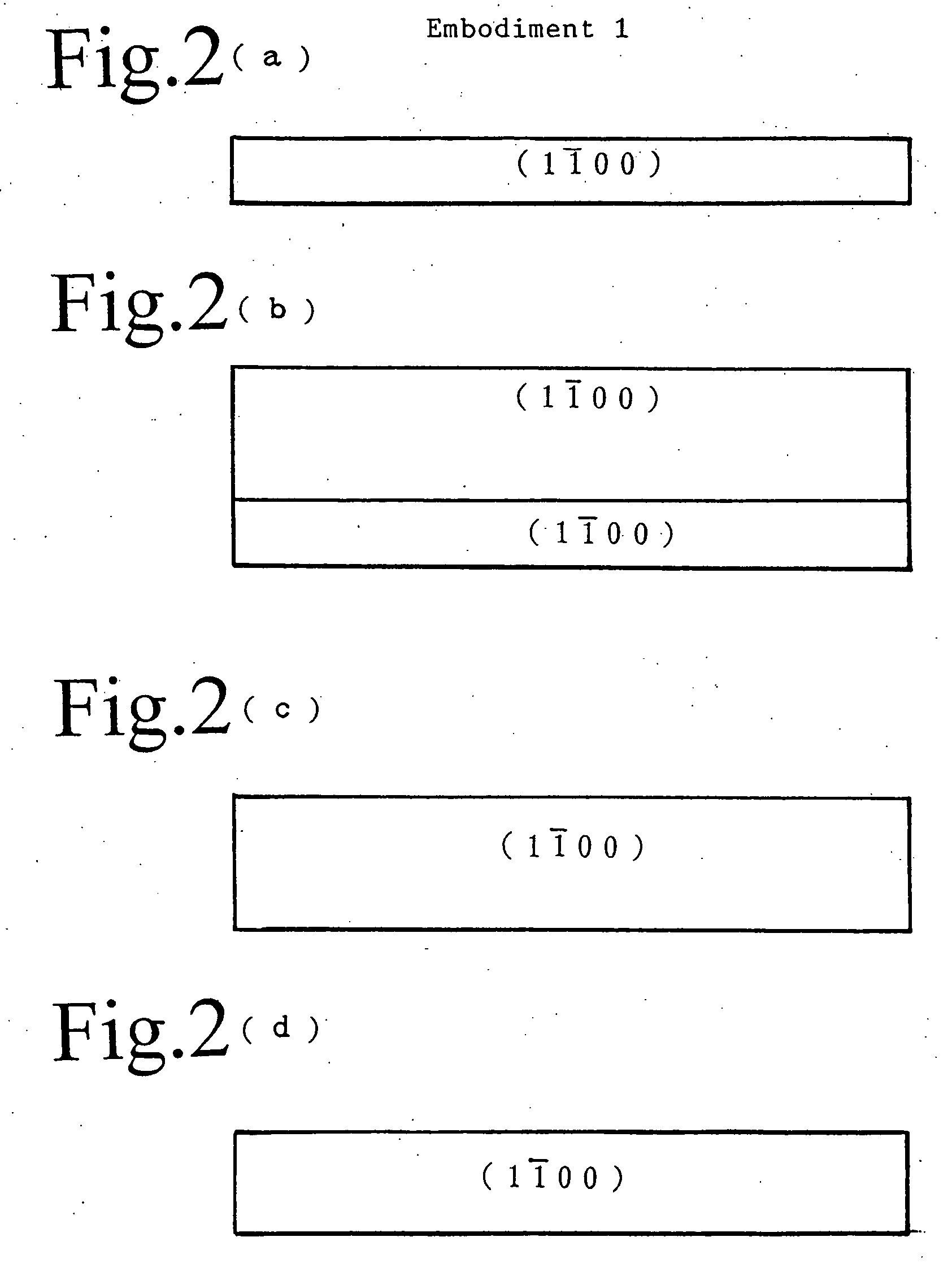
embodiment 1 (m (1-100) surfaced gan crystal seed ; fig.2)

[Embodiment 1 (M (1-100) Surfaced GaN Crystal Seed; FIG. 2)]

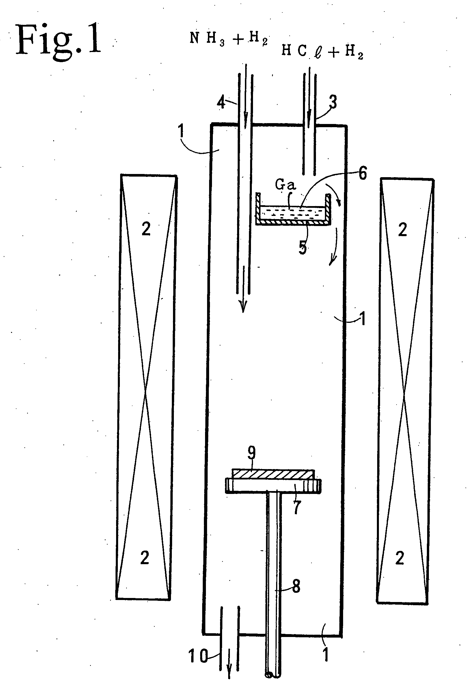
[0085] An M (1-100) plane GaN single crystal is prepared as a seed for putting Method (A) into practice by slicing a bulk GaN single crystal in the planes parallel with an M (1-100) plane (FIG. 2(a)). The M-plane seed crystal has a (1-100) top surface and a (-1100) bottom surface. The bulk GaN single crystal was obtained by growing a thick GaN single crystal upon a (111) GaAs substrate by a lateral overgrowth method and removing the GaAs substrate by solving with aqua regia. The slicing direction M (1-100) is one of planes parallel with a growth direction . The sliced M-surface crystal is polished. The prepared M-plane seed crystal has a flat smooth surface which is immune from degraded superficial layers.

[0086] An HVPE (hydride vapor phase epitaxy) method grows a gallium nitride crystal on the M-plane GaN seed crystal under the following condition.

growth temperature1020° C.NH3 partial pressure0.2 atm (2 × 10⁴ Pa)HCl par...

embodiment 2 (faceted c-plane (0001) gan growth ; fig.4)

[Embodiment 2 (Faceted C-Plane (0001) GaN Growth; FIG. 4)]

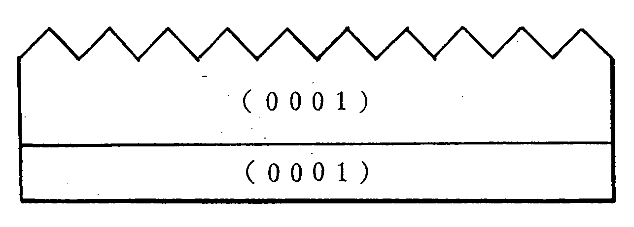
[0103] A C (0001) plane GaN single crystal is prepared as a seed by slicing a bulk GaN single crystal in the planes parallel with a C (0001) plane (FIG. 4(a)). The C-plane seed crystal has a (0001) top surface and a (000-1) bottom surface. The top surface of the GaN seed is a (0001)Ga plane like Comparison Example 1. The sliced C-surface crystal is polished. The prepared C-plane seed crystal has a flat smooth surface which is immune from degraded superficial layers.

[0104] A faceted GaN crystal is grown in the c-direction on the C-plane GaN seed by an HVPE (hydride vapor phase epitaxy) method without eliminating facets under the following condition.

growth temperature1030° C.NH3 partial pressure0.2 atm (2 × 10⁴ Pa)HCl partial pressure1 × 10−2 atm (103 Pa)growth time5 hoursGaN layer thicknessabout 500 μm

[0105] The NH3 material gas includes 2 ppm of water (H2O). Water is added to the NH3 gas intentionally as an oxygen source. ...


PUM

PropertyMeasurementUnit
thicknessaaaaaaaaaa
diameteraaaaaaaaaa
thicknessaaaaaaaaaa

Abstract

Oxygen can be doped into a gallium nitride crystal by preparing a non-C-plane gallium nitride seed crystal, supplying material gases including gallium, nitrogen and oxygen to the non-C-plane gallium nitride seed crystal, growing a non-C-plane gallium nitride crystal on the non-C-plane gallium nitride seed crystal and allowing oxygen to infiltrating via a non-C-plane surface to the growing gallium nitride crystal. Otherwise, oxygen can be doped into a gallium nitride crystal by preparing a C-plane gallium nitride seed crystal or a three-rotationally symmetric plane foreign material seed crystal, supplying material gases including gallium, nitrogen and oxygen to the C-plane gallium nitride seed crystal or the three-rotationally symmetric foreign seed crystal, growing a faceted C-plane gallium nitride crystal having facets of non-C-planes on the seed crystal, maintaining the facets on the C-plane gallium nitride crystal and allowing oxygen to infiltrating via the non-C-plane facets to the gallium nitride crystal.

Description

BACKGROUND OF THE INVENTION [0001] 1. Field of the Invention [0002] This invention relates to an oxygen doping method into a gallium nitride crystal and an oxygen-doped n-type gallium nitride single crystal substrate for producing light emitting diodes (LEDs), laser diodes (LDs) or other electronic devices of groups 3 and 5 nitride semiconductors. Nitride semiconductors means GaN, InGaN, InAlGaN and so on which are grown as thin films on a sapphire substrate. An activation layer is a GaInN layer. Other parts are mainly GaN layers. Thus, the light emitting diodes based upon the nitride semiconductors are represented as GaN-LEDs or InGaN-LEDs which mean the same LEDs. [0003] This application claims the priority of Japanese Patent Application No. 2001-113872 filed on Apr. 12, 2001 which is incorporated herein by reference. [0004] 2. Description of Related Art [0005] Light emitting devices making use of nitride semiconductors have been put on the market as blue-light LEDs. At present, a...

Claims


Application Information

Patent Timeline
Patent Type & Authority Applications(United States)
IPC IPC(8): H01L29/207C30B23/00C30B23/02C30B25/00C30B25/02C30B29/38C30B29/40C30B33/00H01L21/20H01L21/205
CPCC30B23/00C30B23/02C30B25/00C30B25/02C30B29/403C30B29/406C30B29/60C30B33/00H01L21/02389H01L21/02395H01L21/02433H01L21/0254H01L21/02576H01L21/02609H01L21/0262H01L29/2003H01L29/207
Inventor MOTOKI, KENSAKUUENO, MASAKI
Owner SUMITOMO ELECTRIC IND LTD
Why Eureka
Try Eureka