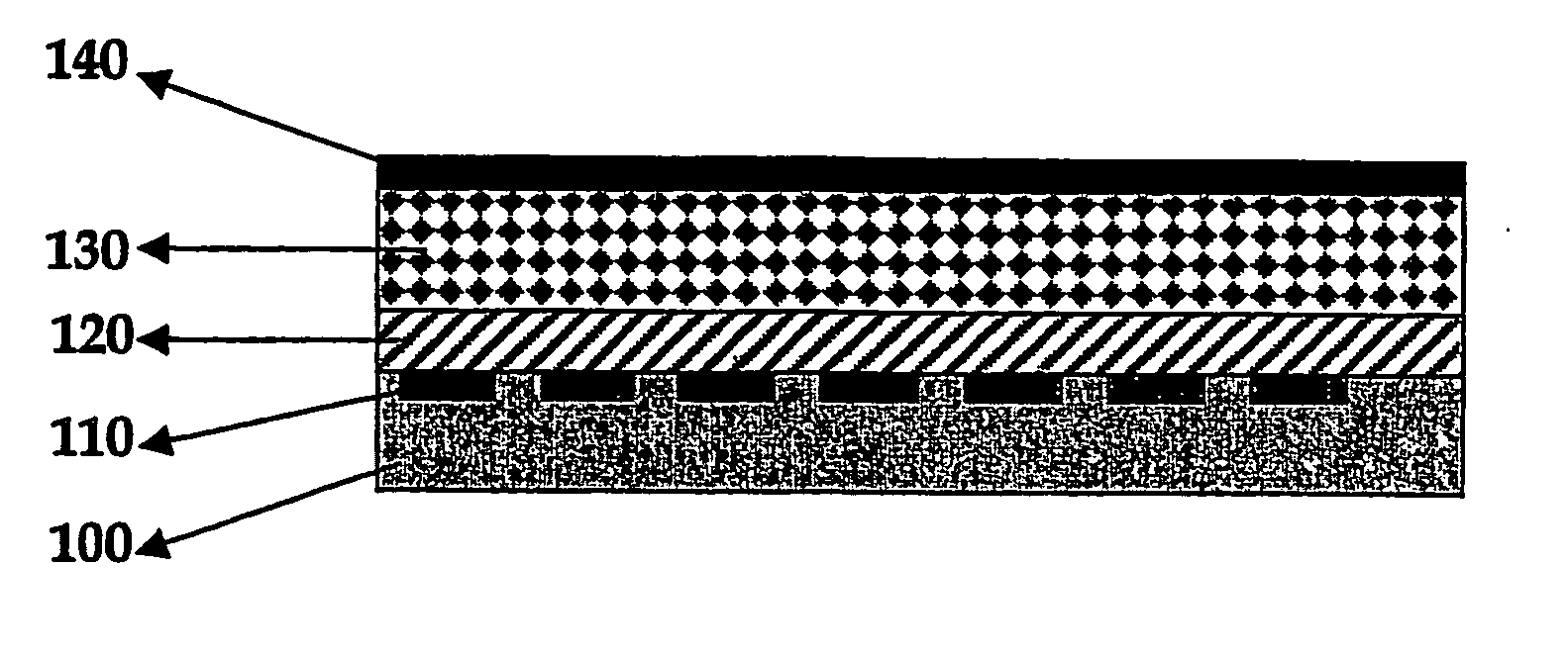
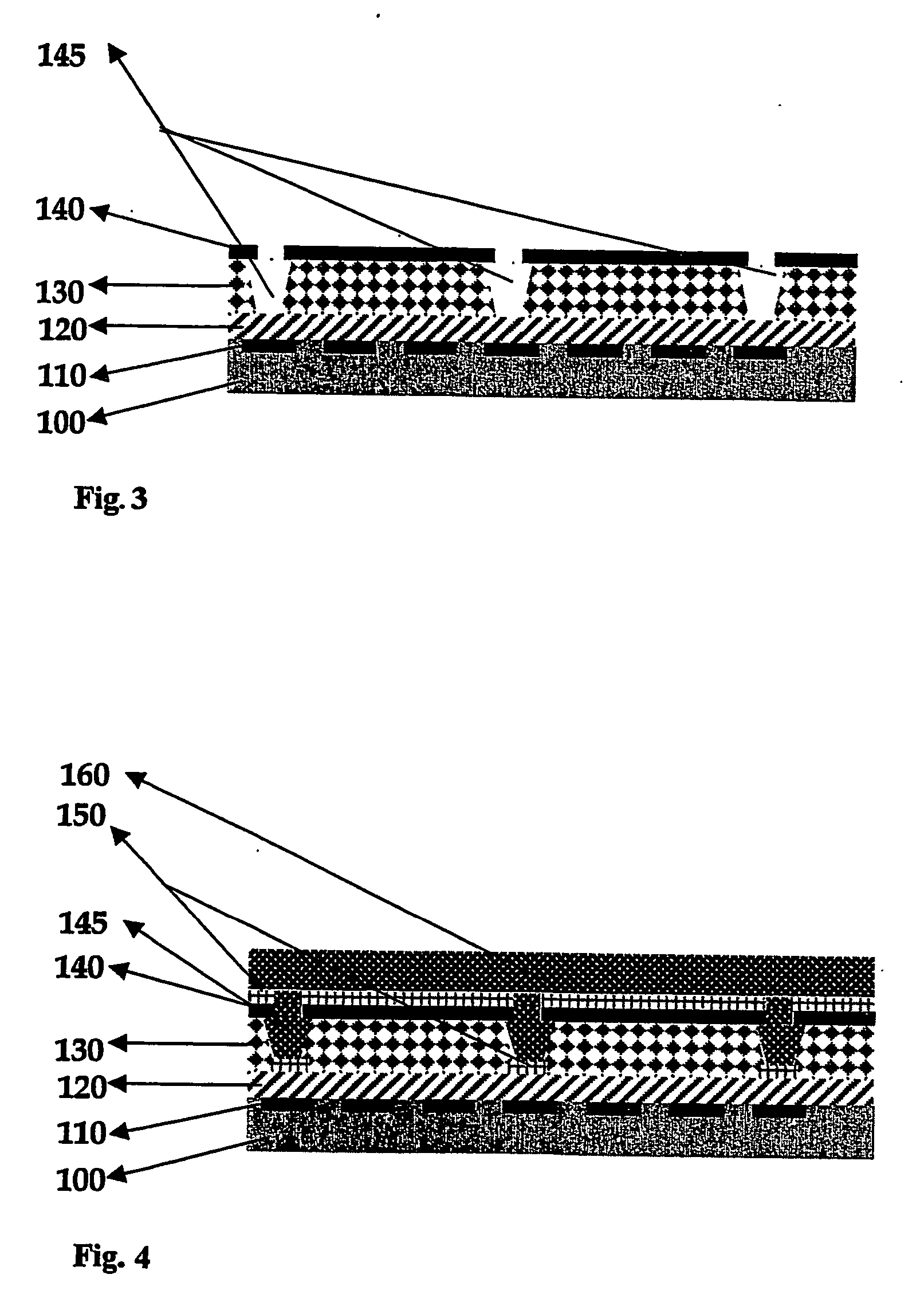
Although substantial progress has been made in the development of full-color PLED displays, additional challenges remain.
However, the main obstacle to overcome here is the compatibility of the solvents for the red, green and blue polymers.
An additional problem related to organic light emitting materials is that they are very delicate and cannot be directly exposed to any
processing steps such as
plasma etching or UV
radiation without suffering severe damage.
Process induced damages reduce the device lifetime, decrease the
photoluminescence efficiency and
quantum efficiency of the device and lead to generally not acceptable device performance.
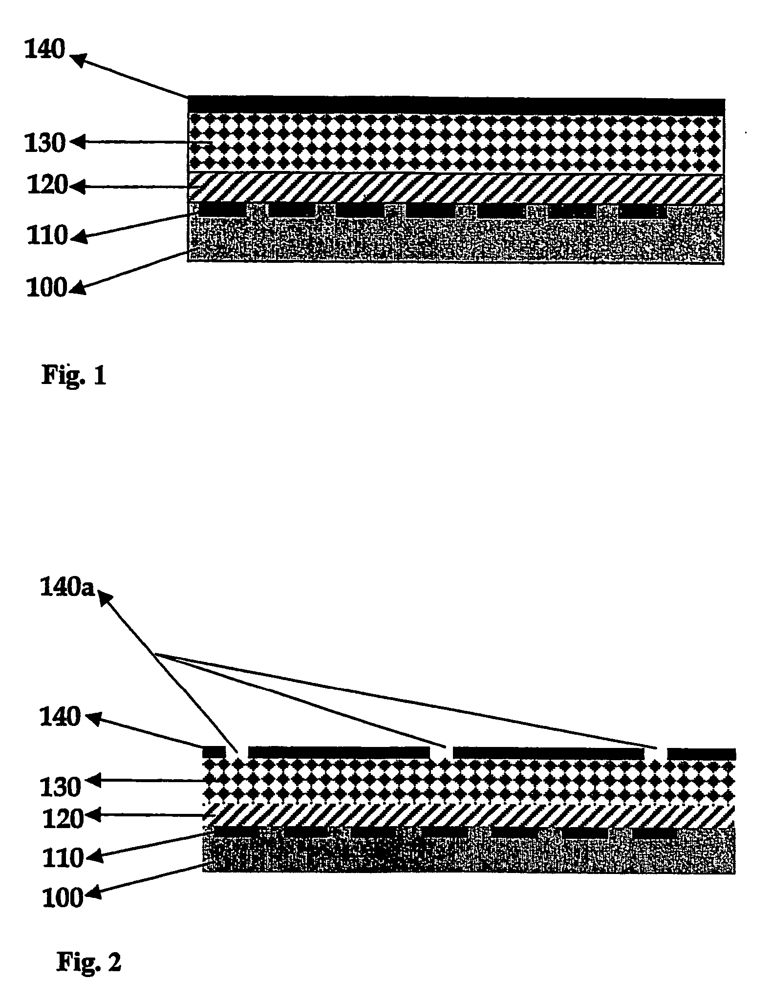
However, inkjet technology is currently only applicable to displays with pixel sizes of greater than 30 micrometers.
Therefore producing displays with a
pitch of 10 micrometers is not possible, as one droplet would automatically cover three pixels.
Other problems related to ink-jet printing in such small dimensions are
volume control of the droplets, placement accuracy of the
polymer droplet and the positioning accuracy of the ink-jet print
nozzle.
The
disadvantage of this approach is that color filters absorb a significant proportion of the initially emitted light and are therefore very inefficient
Another problem with this approach is that efficient color conversion materials that can be patterned to 4-5
micrometer size are, to our knowledge, not readily available.
This process could be used to define pixels for a
monochrome display but it is not suitable for
full color display application, as it does not describe a method for avoiding
contamination of the light emitting polymers during
processing and it does not avoid
polymer mixing.
This process is applicable to produce
monochrome displays but does not lend itself to the production of
full color RGB displays as it is only able to pattern the
cathode and not the light emitting material.
Another drawback of this process is that it does not work very well with top emitting
active matrix displays that require transparent, highly reactive,
low work function thin film cathodes from materials like
calcium,
magnesium etc.
These materials do not lend themselves to the
cold welding process because they react very aggressively and form oxides or nitrides at the interfaces that prevent an effective
cold welding process.
This process again allows the fabrication of
monochrome displays but it does not allow the production of
full color displays as the deposition of a second polymer via
spin coating would dissolve or damage the already patterned pixels.
However, for
solution processed organic light emitting materials such as most conjugated polymers e.g. poly(
phenylene vinylene) (PPV), polyfluorenes, etc this process will not work Most conjugated polymers that are currently used in the field of organic light-emitting displays are soluble in non-polar
aromatic solvents.
This would lead to ill-defined device characteristics and very likely to a complete
device failure.
Such damage is not acceptable to any electro-
optically active material as employed in the field of organic light emitting diodes and polymer
electronics.
Any damage will alter the properties of the organic materials in an ill-defined manner and will have undesired consequences on both lifetime and performance.
However, this process cannot be used for a pattering process of organic electro-
optically active material like light emitting diodes.
This process is also not applicable to patterning organic light emitting polymers, as it gives no clue as to how to overcome the compatibility problems of the
solvent in which the light emitting polymers are dissolved.
The suggested process of
plasma etching will lead to unrecoverable damage of the light-emitting polymer.
The discussion above emphasizes an existing problem in the production of full color display.
One can either apply a uniform single
coating of a light emitting polymer from a solution via
spin coating and pattern it using various techniques to achieve
high resolution monochrome devices and then convert the light via color filters or color changing materials but with the consequent light loss; or selectively deposit individual polymer color elements via e.g.
inkjet printing but then have a more expensive and less scalable process for volume production that does not lend itself to pixel sizes below 30 μm.

