Sputtered transparent conductive films

a technology of transparent conductive films and sputtering methods, which is applied in the direction of electrolysis components, vacuum evaporation coatings, coatings, etc., can solve the problems of difficult switching, high target cost, and difficult so as to facilitate switching, easy selection of surface area, and convenient availability

Inactive Publication Date: 2006-06-08
NEW MILLENNIUM SOLAR EQUIP CORP
View PDF5 Cites 34 Cited by
  • Summary
  • Abstract
  • Description
  • Claims
  • Application Information

AI Technical Summary

Benefits of technology

[0011] Advantageously, the method of the invention uses in one variation metal wires as the dopant target. Such wires are both readily available and inexpensive. Moreover, the ratio of the surface area of the wire to the internal area of the main cathode targets are automatically in an appropriate range for doping (at the level of a few atomic percent). Utilization of wire circumvents the need for machining a planar target to a specific size as is often required in sputtering methods and apparatus. The use of wire offers numerous other advantages which include easy selection of the surface area of the wire by choice of wire diameter, ease of switching between dopants by simply changing the wire, no active cooling of the wire is required (provided it is a refractory metal, or provided it is operated below its melting point). Finally, the apparatus and methods of the invention result in a more effective substitution and doping process. Although not limiting the invention to any particular mechanism for this improvement, dopant atoms in passing through the intense hollow cathode discharge are likely to be activated thereby having sufficient energy for doping. Finally, because of the proximity of the high plasma density in the hollow cathode the present invention allows for dopant material to be sputtered as lower voltages and at higher current densities than can be achieved in conventional non-magnetron sputtering.
[0012] In another embodiment of the invention, an alternative cathode design for use in the sputter apparatus set forth above is provided. In one aspect, this alternative design is mounted on a chamber flange for easy installation and removal from a vacuum chamber. In another aspect, this alternative cathode design includes a reactive gas channel that is integral to the cathode such that the reactive gas is introduced into the sputter-coating system at a position proximate to the flow exit.

Problems solved by technology

The introduction of dopant atoms into materials such as transparent conducting oxides (“TCOs”) presents several technical difficulties.
Such targets are expensive.
However, cross-contamination of the targets seem unavoidable in such designs.
However, there is no flexibility in choice of dopant ratio.
Furthermore, in both cases (dual and separate target cases), oxygen would react with the dopant target or portion of target resulting in a reduced sputter yield and an unpredictable sputtering rate.
However, little is known about the titanium doping of indium oxide.
However, some researchers were unable to obtain doping with Ti.
However, this material has only the modest carrier mobility of ZnO which leads to an inadequately small free carrier absorption.

Method used


Image

  • Sputtered transparent conductive films
  • Sputtered transparent conductive films
  • Sputtered transparent conductive films

Examples


Embodiment Construction

)

[0019] Reference will now be made in detail to the presently preferred compositions or embodiments and methods of the invention, which constitute the best modes of practicing the invention presently known to the inventors.

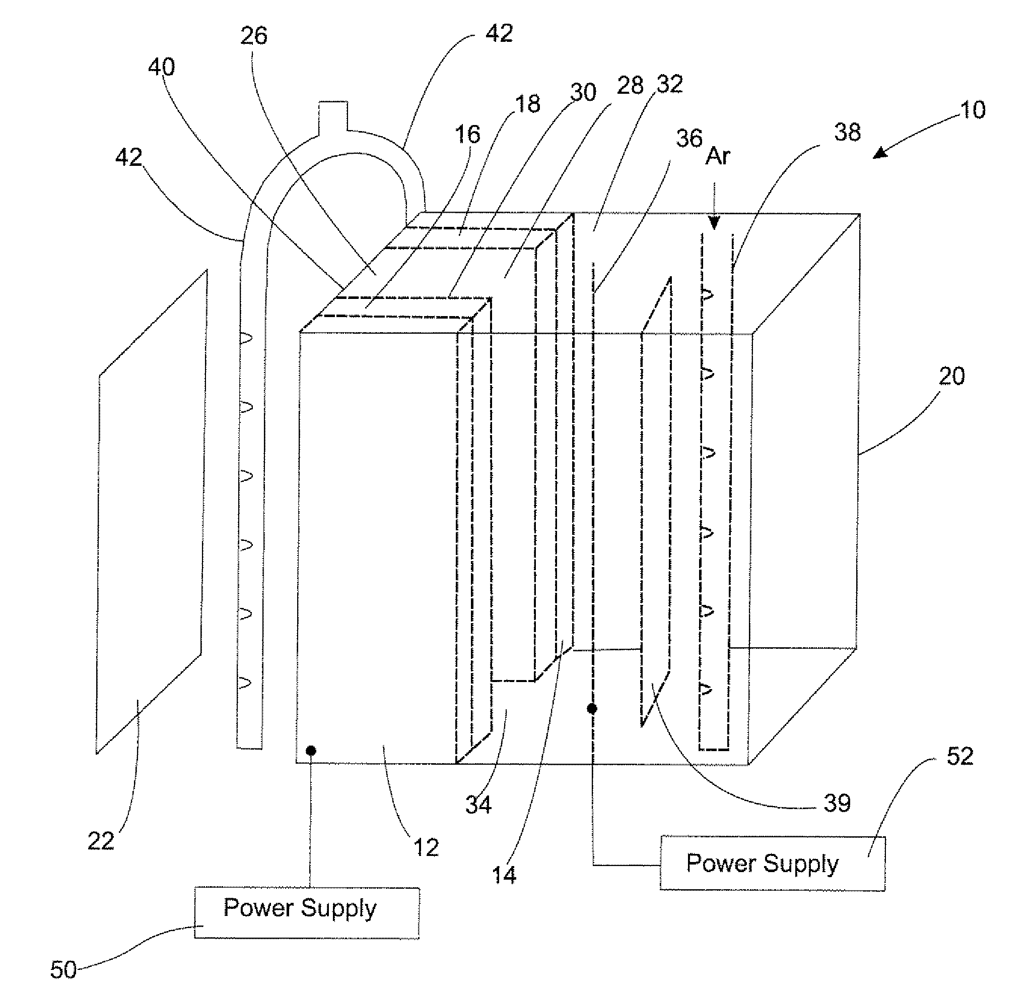
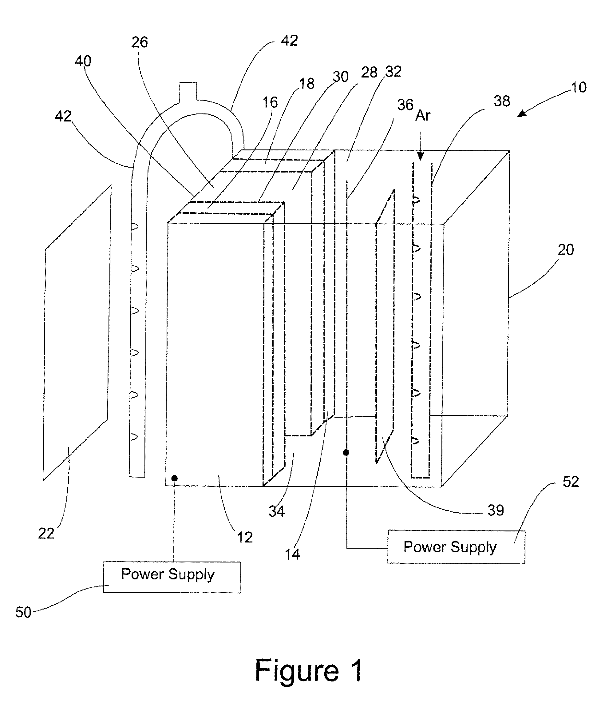
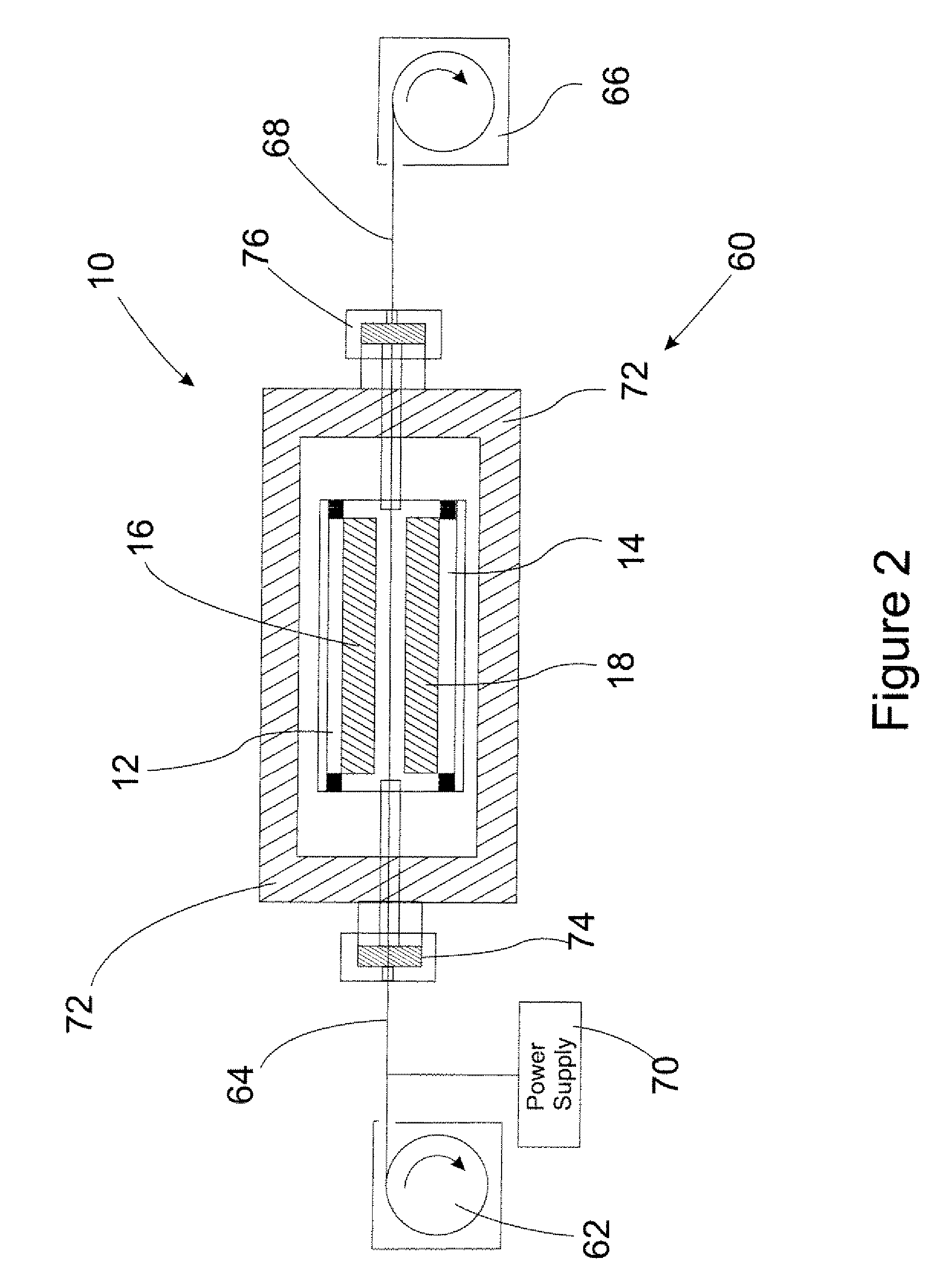
[0020] With reference to FIG. 1, a schematic of the sputter apparatus for introducing doping elements into a coating applied to a substrate of the present invention is provided. Sputtering apparatus 10 includes water cooled cathode sections 12, 14 which are attached to targets 16, 18. Targets 16, 18 are contained with gas box 20. Targets 16, 18 include one or more components that are incorporated into the coating which is sputtered onto substrate 22. Targets 16, 18 typically comprise a metal or metal alloy. Suitable materials included in targets 16, 18 include, for example, zinc, copper, aluminum, silicon, tin, indium, magnesium, titanium, chromium, molybdenum, nickel, yttrium, zirconium, niobium, cadmium, and mixtures thereof. Cathode channel 26 is defined by ma...


PUM

PropertyMeasurementUnit
plasma generatingaaaaaaaaaa
transparent conductingaaaaaaaaaa
concentrationaaaaaaaaaa

Abstract

A hollow cathode sputtering apparatus and related method for introducing dopants into a sputtered coating is provided. The method utilizes a sputter reactor which includes a cathode channel that allows a gas stream to flow therein and a flow exit end from which gases may flow out of and towards a substrate to be coated. The cathode channel as used in the invention is defined by a channel defining surface that includes at least one target material. The sputter reactor further includes a dopant target positioned to provide dopant atoms to the gas stream when the gas stream is flowed through the cathode channel.

Description

CROSS-REFERENCE TO RELATED APPLICATIONS [0001] This application claims the benefit of U.S. provisional application Ser. No. 60 / 634,231 filed Dec. 8, 2004.BACKGROUND OF THE INVENTION [0002] 1. Field of the Invention [0003] The present invention relates to hollow cathode sputtering methods and apparatuses for depositing doped materials on a substrate. [0004] 2. Background Art [0005] The introduction of dopant atoms into materials such as transparent conducting oxides (“TCOs”) presents several technical difficulties. Indium oxide, for example, can be doped by introducing metals such as Sn, Zr, W, Nb, Ti, Mo, and Ta. The dopant atom concentration for optimal doping generally lies somewhere in the 0.5-10 atomic % range. The valence of the host cation in In2O3 is In3+. For a metal to serve as a doping cation it should have a higher valence than that of the host ion for which it substitutes. It is also desirable that it have a diameter equal to or smaller than that of the host ion to suppr...

Claims


Application Information

Patent Timeline
Patent Type & Authority Applications(United States)
IPC IPC(8): C23C14/00
CPCC23C14/086C23C14/228C23C14/3464C23C14/562
Inventor DELAHOY, ALAN E.GUO, SHEYULYNDALL, ROBERT B.SELVAN, J.A. ANNA
Owner NEW MILLENNIUM SOLAR EQUIP CORP
Why Eureka
Try Eureka