Piezoelectric element and method for manufacturing

Inactive Publication Date: 2006-06-22
NAT INST OF ADVANCED IND SCI & TECH
View PDF5 Cites 13 Cited by
  • Summary
  • Abstract
  • Description
  • Claims
  • Application Information

AI Technical Summary

Benefits of technology

[0012] With the structure, the piezoelectric layer of the piezoelectric device is made of aluminum nitride and / or zinc oxide. Aluminum nitride and zinc oxide with a crystal structure have inborn piezoelectric characteristics because their crystal structures are not symmetrical, they do not have Curie temperature unlike ferroelectrics and never make magnetic transition at high temperature, so that they do not lose piezoelectric characteristics until their crystals melt or sublimate. As a result, the piezoelectric layer made of aluminum nitride and / or zinc oxide has high heat-resistance and its piezoelectric characteristics never deteriorate at high temperature. Further, aluminum nitride and zinc oxide are easily processed and suitable to be thin-filmed, so that the piezoelectric device can be small.
[0037] With the structure, the first electrode layer is formed easily. “Physical vapor deposition process” is a process in which a matter is evaporated through physical means, solidified on a part for film formation, and made into a thin film. The process points mainly to a sputtering process, an ion plating process and a vacuum deposition process. Further, with the structure, needle-like shaped crystal pillars of a piezoelectric material grow like frost in the ground, so that the piezoelectric material can form a thin film in a single crystal condition.

Problems solved by technology

But the function of a Peltier element is limited to generating local temperature gradient, so that the sensor cannot be applied to a place where a cooling device cannot be installed on the outside and temperature rises high on the whole.
However, as for a structure with its temperature rising high, as shown above, a usual thin-filmed piezoelectric sensor is inferior in heat-resistance, and so the vibration is to be induced to a distant place at low temperature by a vibration-transmitting stick and measured there.
But in this case, due to reasons such as attenuation of a vibration or mixture of a noise, the vibration of the target of measurement cannot be measured accurately.
But lithium niobate has several faults; it is difficult to be formed as a thin film, it cannot gain piezoelectric characteristics unless it is single crystal, and it is difficult to be fabricated or processed and costs a lot.
However, though thin films made of aluminum nitride or zinc oxide have been made in many processes until now, studies on the degree of dipole-orientation of a thin film made of aluminum nitride or zinc oxide have been hardly done, and therefore there is a problem that it is difficult to fabricate a thin film in which the degree of the dipole-orientation is controlled.
Further, the thin film made of aluminum nitride or zinc oxide has a very large internal stress created in a film forming process, and therefore, for example, in the case of forming the thin film on an electrode made on a substrate, there is a problem that a crack appears in the electrode or the thin film peels off from the substrate, accompanied by the electrode.

Method used


Image

  • Piezoelectric element and method for manufacturing
  • Piezoelectric element and method for manufacturing

Examples


first embodiment

[0039] First embodiment of the present invention is explained below.

[0040] A piezoelectric device according to the present embodiment includes a lamination structure having a lower electrode (a first electrode layer), a piezoelectric thin film (a piezoelectric layer) and an upper electrode (a second electrode layer) successively on a substrate. Because the piezoelectric device according to the present embodiment is a piezoelectric device in which the piezoelectric thin film is formed on the substrate, it can be used as a pressure sensor, a vibration sensor, an acceleration sensor, a surface elastic wave filter, or the like, and besides it can be made highly sensitive.

[0041] As for the substrate, it is possible to use not only a single crystal substrate made of single crystal such as sapphire or silicon, but also a substrate other than a single crystal substrate, such as a glass substrate, a polycrystalline ceramic substrate, a metal substrate or a resin substrate. As mentioned lat...

second embodiment

[0060] Second embodiment of the present invention is explained below.

[0061] A piezoelectric device of the present embodiment has a lower electrode that is a laminated body including a contact layer for contacting closely with a substrate, and an electrode layer (a conducting layer) as an electrode. As for other structures, they are the same as the piezoelectric device explained in the first embodiment.

[0062] A surface layer of the lower electrode, that is a laminated body, contacts with a piezoelectric thin film. Aluminum nitride and / or zinc oxide that forms the piezoelectric thin film can, just like the first embodiment, have a high degree of dipole-orientation on a metal whose electronegativity ranges, for example, from 1.3 to 1.5, and therefore it is more desirable that a metal that forms the surface layer of the lower electrode is a metal whose electronegativity ranges from 1.3 to 1.5. Further, it is more desirable that the metal that forms the surface layer of the lower elect...

examples

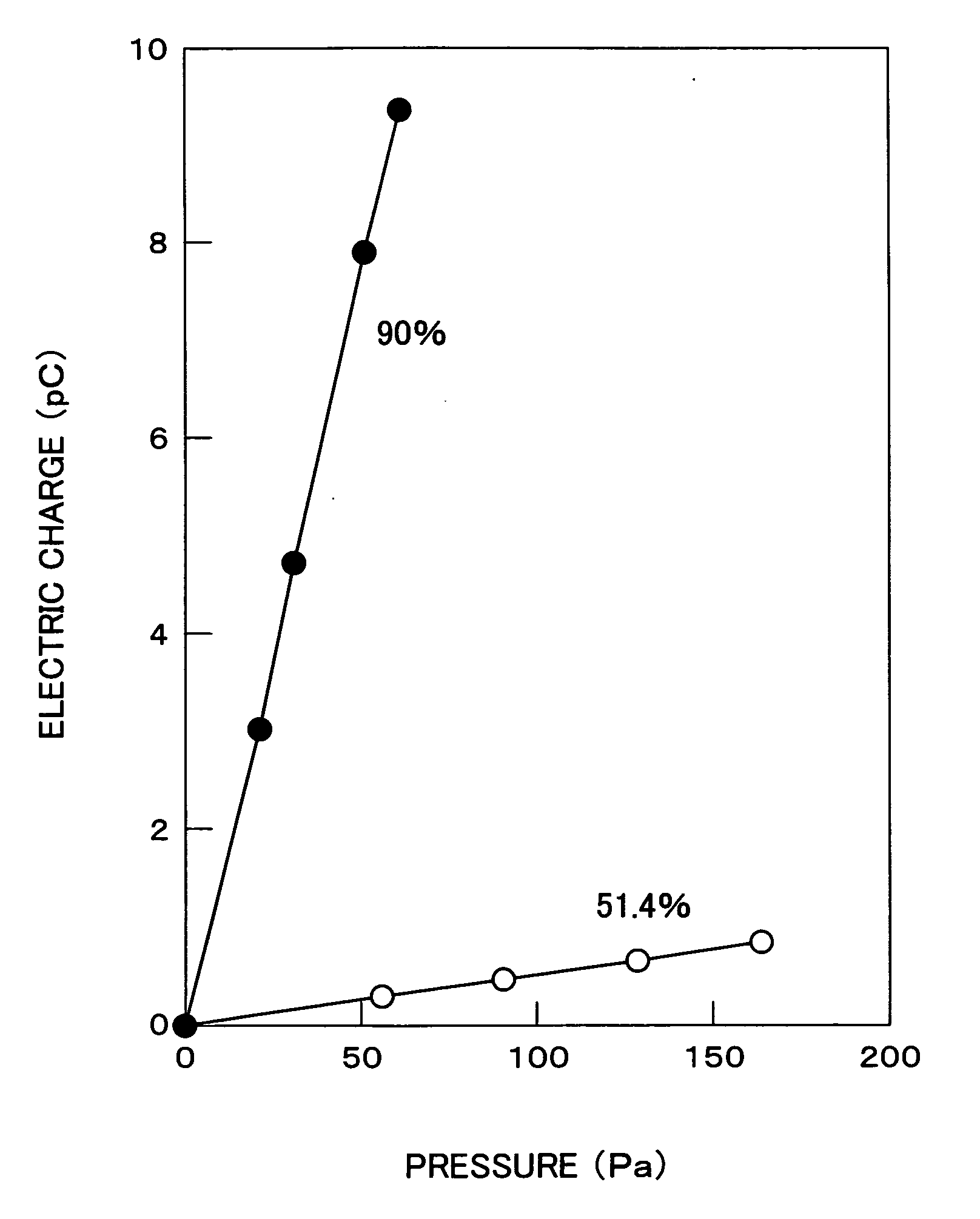
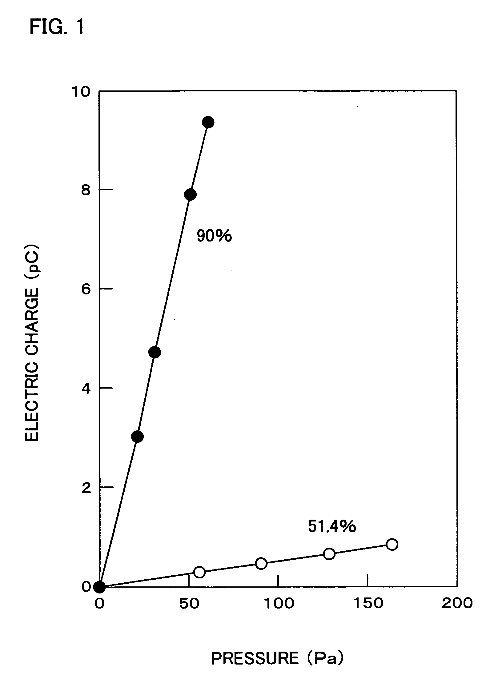
[0074] It is known that electric characteristics of a piezoelectric device, such as an electromechanical coupling coefficient, greatly depend on the degree of dipole-orientation of a piezoelectric thin film. Therefore, in order to provide a piezoelectric device with a piezoelectric thin film that has a higher degree of dipole-orientation, the influence of a lower electrode on the formation of a piezoelectric thin film, and the effect of making a lower electrode a laminated body in the formation of a piezoelectric thin film, were examined. The details are explained below.

(The Influence of a Lower Electrode)

[0075] Examples of past main studies in which an aluminum nitride thin film was formed on a conductor, are as follows; a study for increasing corrosion-resistance of iron, and a study in which an aluminum nitride thin film was formed on an aluminum electrode for an SAW (surface acoustic wave) filter. Studies in which an aluminum nitride thin film was formed on other kinds of con...


PUM


Abstract

A lower electrode is formed on a silica glass substrate or a stainless substrate. Through a sputtering process, a thin film of aluminum nitride and / or zinc oxide is formed on the lower substrate so that the degree of dipole-orientation becomes 55% or more, and thereby a piezoelectric thin film is formed. And an upper electrode is formed on the piezoelectric thin film. A piezoelectric device has a piezoelectric layer made of aluminum nitride and / or zinc oxide. Aluminum nitride and zinc oxide with a crystal structure have inborn piezoelectric characteristics because their crystal structures are not symmetrical, they do not have Curie temperature unlike ferroelectrics, and in aluminum nitride and zinc oxide, magnetic transition does not occur even at high temperature, so that they never lose piezoelectric characteristics until crystal melts or sublimates.

Description

TECHNICAL FIELD [0001] The present invention relates to a piezoelectric device and a fabrication method thereof. Particularly, the present invention relates to a piezoelectric device made of a thin film in which aluminum nitride and / or zinc oxide is highly dipole-orientated on a substrate, and to a fabrication method thereof. BACKGROUND ART [0002] Conventionally, in order to sense abnormality of a structure that generates atmosphere of high temperature, such as a conduit or a valve of a plant (e.g. a nuclear power plant), or an internal combustion engine, a sensor is put inside the structure. Examples of the sensor are as follows; an acoustic emission sensor for sensing an acoustic emission that is an elastic wave generated when a crack or a crevice is made, and a piezoelectric vibration sensor for sensing information of an abnormal vibration or acceleration. As the examples of these sensors, a compressed type, a cantilevered type, a diaphragm type, and a shearing type are known. [0...

Claims


Application Information

Patent Timeline
IPC IPC(8): H01L29/84H01L41/09G01H11/08H01L41/18H01L41/187H01L41/22H01L41/29H01L41/316H01L41/319H03H9/17
CPCH01L41/316H10N30/076H10N30/20H10N30/85H10N30/01
Inventor AKIYAMA, MORITOUENO, NAOHIROTATEYAMA, HIROSHIKUWANO, NORIYUKI
Owner NAT INST OF ADVANCED IND SCI & TECH
Why Eureka
Try Eureka