Electrochemical machining device and electrochemical machining method

a technology of electrochemical machining and electrochemical processing, which is applied in the direction of machining electric circuits, manufacturing tools, electric circuits, etc., can solve the problems of deteriorating workpiece properties, large number of defects, and constant so as to suppress the change of fluid electric conductivity and improve flattening properties

Inactive Publication Date: 2006-07-06
EBARA CORP
View PDF11 Cites 23 Cited by
  • Summary
  • Abstract
  • Description
  • Claims
  • Application Information

AI Technical Summary

Benefits of technology

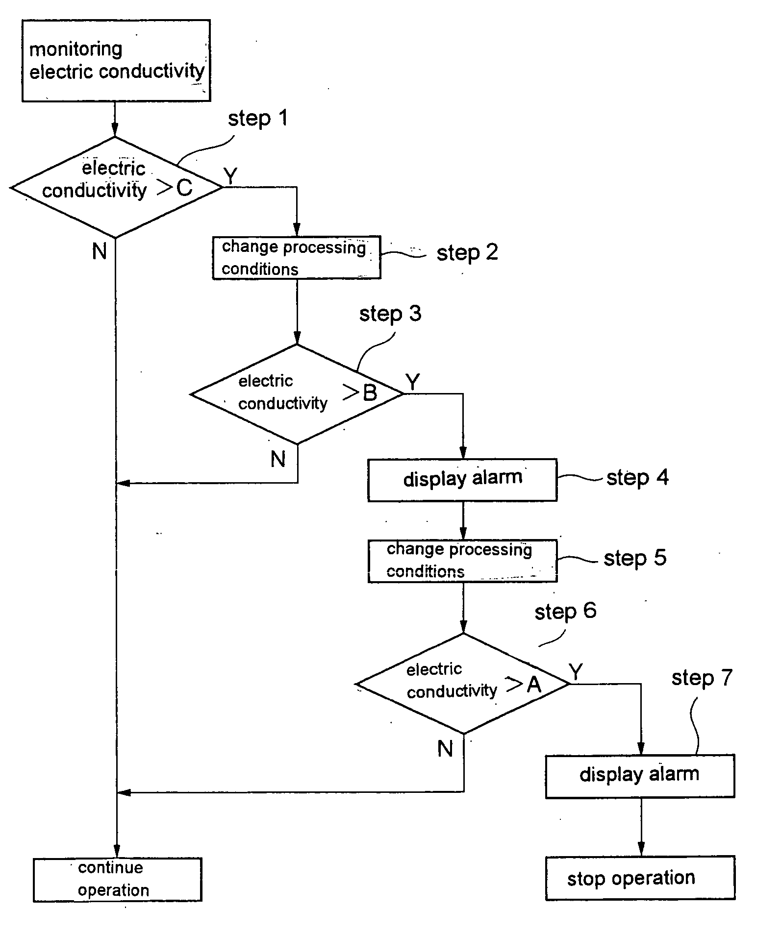
[0034] The present invention has been made in view of the above situation in the background art. It is therefore a first object of the present invention to provide an electrolytic processing apparatus and an electrolytic processing method which can suppress a change in the electric conductivity of a fluid due to contaminants, such as processing products, produced upon the electrolytic processing, so that the fluid can maintain good flattening properties.

Problems solved by technology

Under these circumstances, in such a conventional machining method that a desired portion in a workpiece is physically destroyed and removed from the surface thereof by a tool, a large number of defects may be produced to deteriorate the properties of the workpiece.
In fact, however, the electric conductivity of the fluid is always changing due to contaminants, such as processing products of the electrolytic processing, scrapings of an ion-exchange membrane, metal ions (e.g. copper ions), and additives.
With these processing methods, however, application of a mechanical force to a workpiece may cause defects in the workpiece, impairing the properties of the workpiece.
For instance, when buffing an aluminum member, polishing particles can be embedded in the surface of the soft workpiece, making it difficult to obtain a specular finish.
A polishing pad, after its repeated use, loses its proper roughness and also its polishing effect.
With the recent movement toward higher integration of devices in the field of semiconductor industry, however, there is a tendency to use as an insulating film a porous low-k material which has a very low mechanical strength.
Such an insulating film having a very low mechanical strength can be easily destroyed with the pressing force of a polishing pad during CMP processing.
According to electrolytic processing, therefore, defects in a workpiece caused by its plastic deformation, such as a damager layer and dislocation, are not produced.
CMP using a slurry (suspension containing abrasive grains) generally employs an operation of pressing a metal, and therefore involves the problem of causing defects, such as dishing, erosion and recesses, in the processed surface of the metal.
Such chemicals basically increase environmental burden.
Further, when processing a workpiece that requires a high level of purity, such as a semiconductor device, there is a fear of chemical contamination.
However, when pits are formed in a sealing surface of e.g. a vacuum device or a pressure device that requires a high degree of sealing, the desired vacuum or pressure may not be obtained.
Further, the pits can promote corrosion of the metal.
Also in the case of a semiconductor device, the formation of pits may exert various adverse influences.
CMP processing generally necessitates a considerably complicated operation and control, and needs a considerably long processing time.
This also imposes a considerable load on the slurry or cleaning liquid waste disposal.
Also in this connection, it is to be pointed out that though a low-k material, which has a low dielectric constant, is expected to be predominantly used in the future as a material for the insulating film, the low-k material has a low strength and therefore is hard to endure the stress applied during conventional CMP processing.
According to this process, the machining is carried out to the growing surface of a plating film and promotes an abnormal deposition of plating, causing the problem of denaturing of the resulting film quality.
Further, when a fragile material, such as a low-k material, is processed in a semiconductor device manufacturing process, there is a fear of destruction of the material due to buckling, etc.
It is therefore not possible with such a processing as CMP to apply a high surface pressure between a substrate and a polishing surface, whereby a sufficient polishing cannot be performed.
The above problem becomes remarkable when such a fragile material is used.
It is however possible that a surface pressure is produced when a substrate is brought into contact with a processing electrode, which could cause destruction of a semiconductor device.
In the case where a processing electrode and a feeding electrode are disposed opposite to the workpiece, because of the presence of fine residues between the processing electrode, the feeding electrode and the workpiece, it becomes difficult for the processing electrode and the feeding electrode to make contact with the workpiece, so that it is likely that the processing does not progress smoothly and the amount of residues increases.
The residues or extraneous matter, such as a processing product, an unreacted residual metal, etc., adsorbed as contaminants on a workpiece during the conventional electrolytic processing, can lower the reliability of the product (processed workpiece).
Especially in the case of a semiconductor device, such residues can lead to short-circuit between interconnects, etc., and thus adversely affect the reliability of the device.

Method used


Image

  • Electrochemical machining device and electrochemical machining method
  • Electrochemical machining device and electrochemical machining method
  • Electrochemical machining device and electrochemical machining method

Examples


example 1

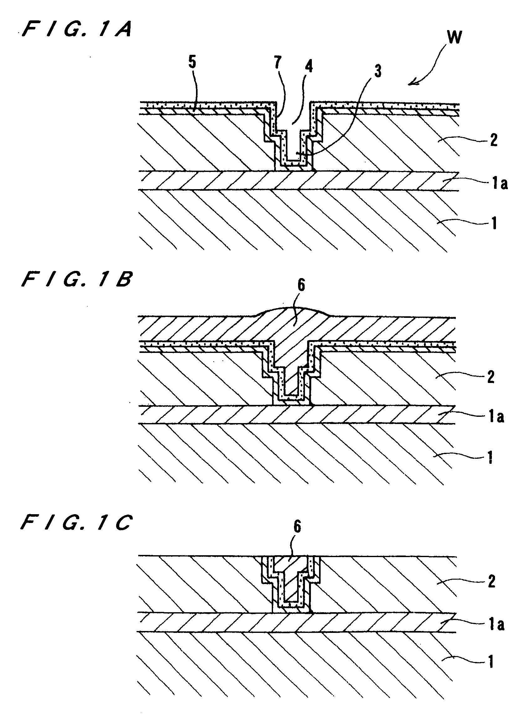
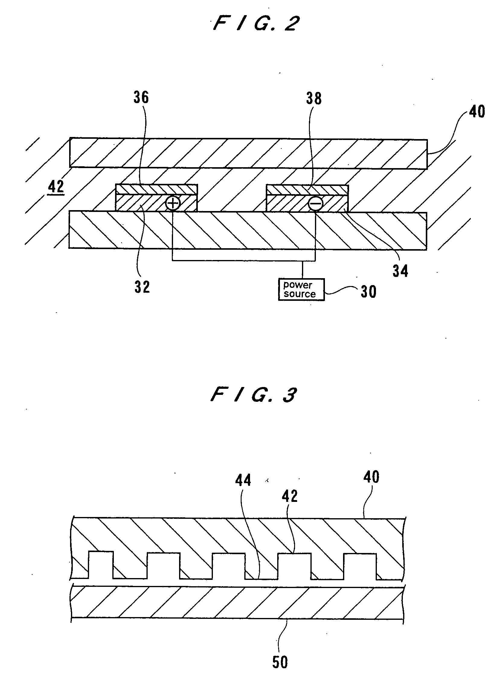
[0276] A sample (workpiece) for electrolytic processing was prepared by forming a 1.5 μm thick copper film by electroplating on a wafer having a diameter of 20 cm. A current-carrying portion of a platinum plate, on which a diaphragmatic ion exchanger and a porous ion exchanger are superimposed, was used as a processing electrode. Nafion 117 (trademark, DuPont Co.) was used as the diaphragmatic ion exchanger; a polyethylene non-woven fabric having a sulfonic ion-exchange group, introduced by graft polymerization, was used as the porous ion exchanger. The processing electrodes and the wafer were sunk in a water tank filled with ultrapure water, and the wafer was rotated at 500 rpm by a rotating machine. The processing electrodes were connected to a cathode of a bipolar power source, while a brash electrode (feeding electrode) was connected to an anode, and the brash electrode was brought into contact with the rotating wafer. The lowest potential of the bipolar power source was set at ...

example 2

[0277] A sample (workpiece) for electrolytic processing was prepared by forming a 1.5 μm thick copper film by electroplating on a wafer having a diameter of 20 cm. A processing electrode was composed of a diaphragmatic ion exchanger, a porous ion exchanger and a current-carrying portion of a platinum plate. Nafion 117 was used as the diaphragmatic ion exchanger; a polyethylene non-woven fabric having a sulfonic ion-exchange group, introduced by graft polymerization, was used as the porous ion exchanger. The processing electrodes and the wafer were sunk in a water tank filled with ultrapure water, and the wafer was rotated at 500 rpm by a rotating machine. The processing electrodes were connected to a cathode of a bipolar power source, while a brash electrode (feeding electrode) was connected to an anode, and the brash electrode was brought into contact with the rotating wafer. The pulse wave of the bipolar power source was set in a constant current mode such that an electric current...

example 3

[0278] A sample (workpiece) for electrolytic processing was prepared by forming a 1.5 μm thick copper film by electroplating on a wafer having a diameter of 20 cm. A processing electrode was composed of a diaphragmatic ion exchanger, a porous ion exchanger and a current-carrying portion of a platinum plate. Nafion 117 was used as the diaphragmatic ion exchanger; a polyethylene non-woven fabric having a sulfonic ion-exchange group, introduced by graft polymerization, was used as the porous ion exchanger. The processing electrodes and the wafer were sunk in a water tank filled with pure water having an electric conductivity of 3 μS / cm, and the wafer was rotated at 500 rpm by a rotating machine. A slidax was provided as a power source. A diode was installed on the output side of the slidax power source in order to cut the negative potential half-waves. The diode output side was connected to a brush electrode, and the brush electrode was brought into contact with the rotating wafer. A f...


PUM

PropertyMeasurementUnit
electric conductivityaaaaaaaaaa
positive potential timeaaaaaaaaaa
electric conductivityaaaaaaaaaa

Abstract

A object of this invention is to provide an electrolytic processing method and apparatus that can suppress a change in the electric conductivity of a fluid due to contaminants, such as processing products produced in electrolytic processing, so that the fluid can maintain good flattening properties. The electrolytic processing apparatus of this invention includes: a processing electrode (42) that can come into contact with a workpiece (W); a feeding electrode (44) for feeding electricity to the workpiece (W); a holder (22) for holding the workpiece (W); a power source (26) for applying a voltage between the processing electrode (42) and the feeding electrode (44); a fluid supply section (50) for supplying a fluid between the workpiece (W) and at least one of the processing electrode (42) and the feeding electrode (44); a sensor (80) for measuring the electric conductivity of the fluid; and a control section (84) for changing the processing conditions based on the electric conductivity measured by the sensor (80).

Description

TECHNICAL FIELD [0001] The present invention relates to an electrolytic processing apparatus and an electrolytic processing method, and more particularly to an electrolytic processing apparatus and an electrolytic processing method useful for processing a conductive material formed in a surface of a substrate, such as a semiconductor wafer, or for removing impurities adhering to a surface of a substrate. [0002] The electrolytic processing apparatus and the electrolytic processing method of the present invention are also useful for processing a metal portion of e.g. a vacuum device or high-pressure device that requires a high-precision surface finish, or for removing impurities adhering to a surface of such a workpiece. BACKGROUND ART [0003] In recent years, instead of using aluminum or aluminum alloys as a material for forming circuits on a substrate such as a semiconductor wafer, there is an eminent movement towards using copper (Cu) which has a low electric resistivity and high el...

Claims


Application Information

Patent Timeline
Patent Type & Authority Applications(United States)
IPC IPC(8): B23H7/20B23H3/02B23H5/08B23H9/00
CPCB23H3/02B23H9/00B23H5/08
Inventor KOBATA, ITSUKIKUMEKAWA, MASAYUKINABEYA, OSAMUSERIKAWA, ROBERTO MASSAHIROSAITO, TAKAYUKISUZUKI, TSUKURUKODERA, AKIRAYASUDA, HOZUMIIIZUMI, TAKESHISHIRAKASHI, MITSUHIKO
Owner EBARA CORP
Why Eureka
Try Eureka