Field emitter device

Inactive Publication Date: 2006-11-23
UNIVERSITY OF BRISTOL
View PDF10 Cites 22 Cited by
  • Summary
  • Abstract
  • Description
  • Claims
  • Application Information

AI Technical Summary

Benefits of technology

[0014] The present invention advantageously uses commercially available diamond powders for making the improved cold cathode electron sources (and the resulting emitter structures). The diamond powders are treated to enhance their conductivity, electron affinity and their capability for electron emission upon application of electric fields of 0.5-5V/micron. Specifically, electron emitters containing nanodiamond particles with an average particle size of 25 nm, are heat-treated in an inert atmosphere, subsequently under high vacuum, and with lithium or a lithium compound to produce metal-doped nanodiamond with a controllable hydrogen content. This material is disposed onto a low workfunction, metal alloy cathode contact. Following an air-bake cycle, an emitter structure is formed. The lithium-doped, nan

Problems solved by technology

Furthermore, it is difficult, tedious and expensive to build high densities of field emitters with such fine featured lithography on large area substrates.
The high voltage operation increases damage caused by ion bombardment and surface diffusion on the emitter tips.
The vulnerability of these materials to ion bombardment, chemically active species and temperature extremes is also a serious concern.
However, the n-type doping process has not been reliably achieved for thin film synthetic material.
This has led to alternative methods being disclosed that attempt to produce low voltage operation from diamond by growing or treating it so that the material contain

Method used


Image

  • Field emitter device
  • Field emitter device
  • Field emitter device

Examples


first embodiment

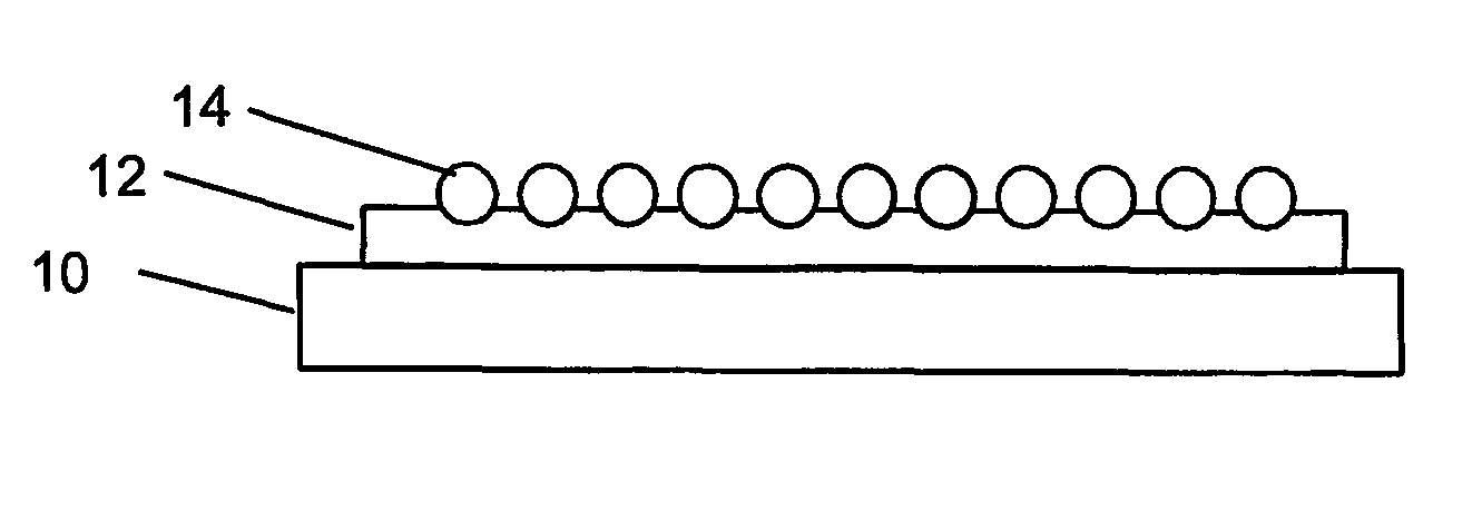
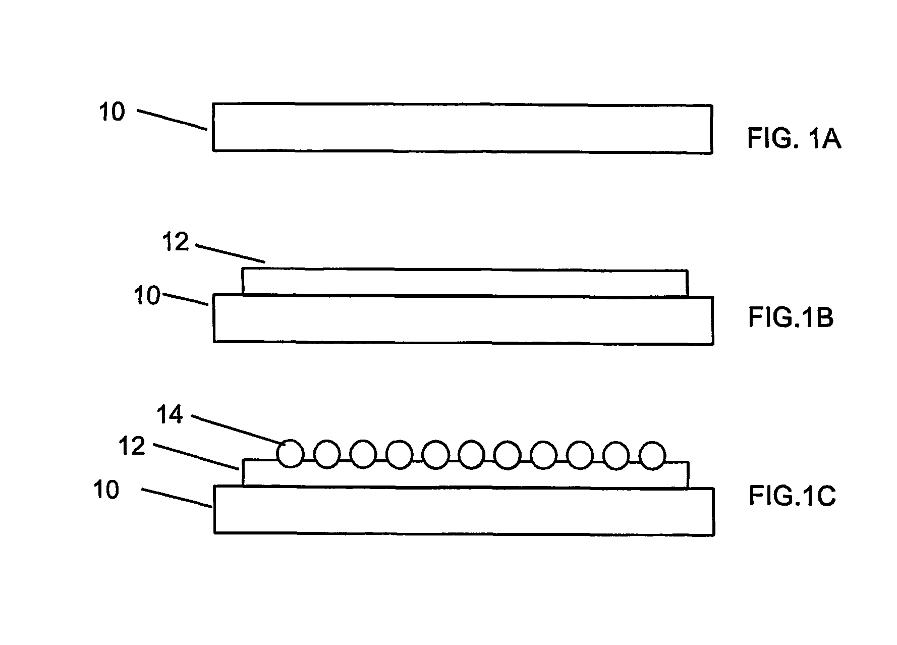
[0028]FIGS. 1A-1C are schematic diagrams showing three successive stages of fabricating a cold cathode emitter in accordance with the present invention. In FIG. 1A, a substrate 10 provides a base upon which emission areas can be fabricated and this substrate 10 is a relatively flat area composed of glass or quartz. Next, as shown in FIG. 1B, a continuous cathode metal layer 12 is deposited upon the substrate. This relatively thin film comprises a metal alloy of approximately 80-120 nm depth (and that is matched to glass). The cathode metal layer 12 can be one of a group of conductive metal oxides such as indium tin oxide (ITO), zinc oxide (ZnO), aluminium-doped zinc oxide (ZnO:Al), indium-doped zinc oxide (ZnO:In), gallium- and aluminium-codoped zinc oxide (ZnO:Ga,Al) or one of a group of metal alloys such as aluminium-doped lithium (Li:Al), silver-doped lithium (Li:Ag), nichrome (Ni—Cr) or one of a group of metals such as silver (Ag), gold (Au), platinum (Pt) and nickel (Ni). A mon...

second embodiment

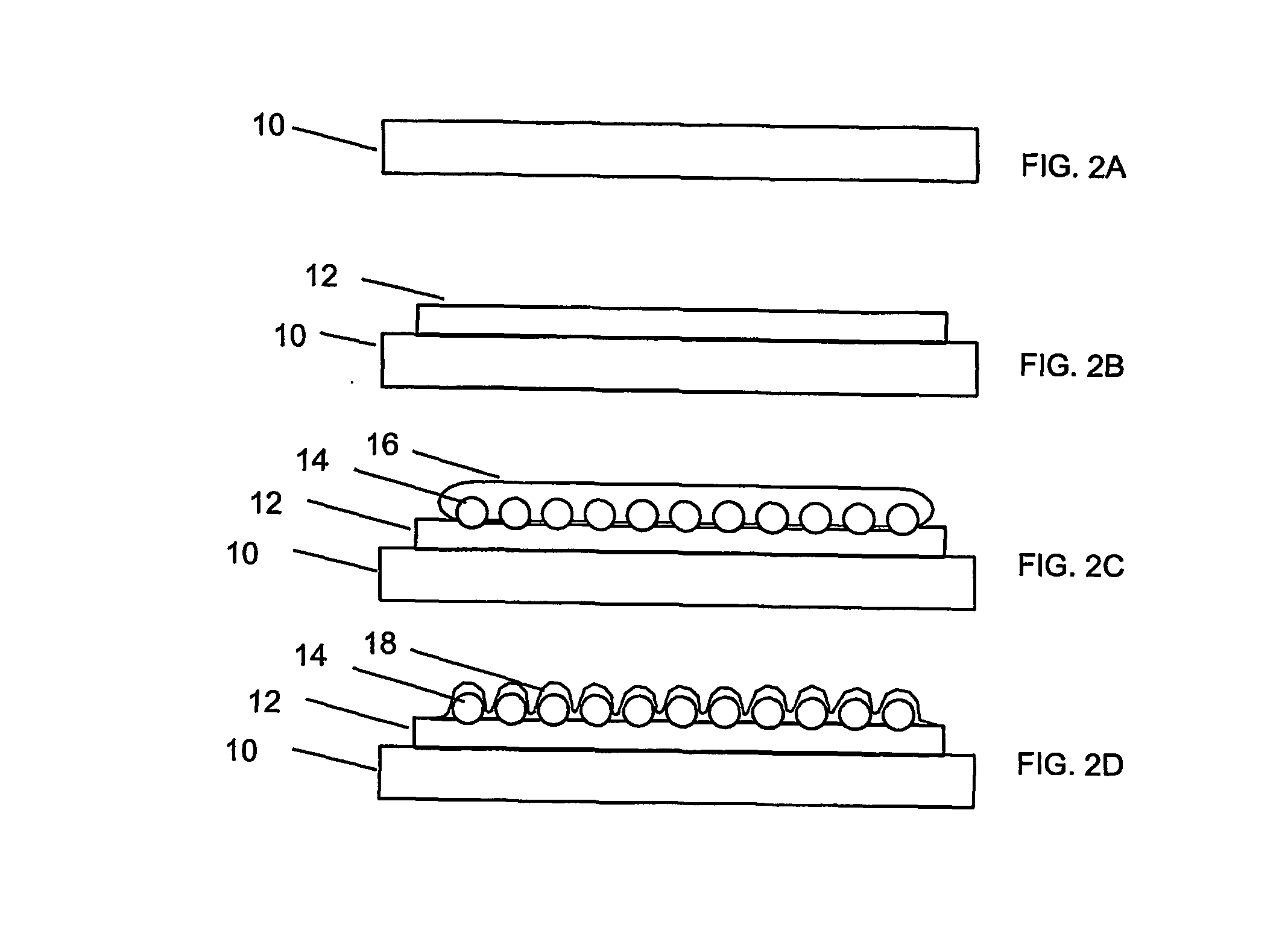
[0030]FIGS. 2A-2D are schematic diagrams showing four successive stages of fabricating a cold cathode emitter in accordance with the present invention. FIG. 2A is similar to FIG. 1A.

[0031] In FIG. 2B, the metal alloy cathode 12 used as the injecting back contact, contains a lithium component and / or an indium component and forms a low resistivity layer when disposed on a supporting substrate 10 and the resistivity value of the cathode 12 does not alter significantly with subsequent substrate processing at elevated temperatures in air. The cathode 12 is deposited on the chemically pre-cleaned substrate surface 10. Evaporation is the preferred deposition technique because it enables large area films to be deposited most easily, with high uniformity, and low levels of included gas. Alternatively, plasma-assisted deposition methods could be used but extra attention needs to be taken to ensure that the deposited metal does not contain large amounts of trapped gas such as argon which is kn...

third embodiment

[0037]FIGS. 3A-3G are schematic diagrams showing seven successive stages of fabricating a cold cathode emitter in accordance with the present invention. FIGS. 3A and 3B are similar to FIGS. 1A and 1B.

[0038] In FIG. 3C a lacquer 20 containing a material such as poly-vinyl acrylic is applied to the cathode 12 as a thin layer by spinning or spraying or printing. In FIG. 3D the lithiated nanodiamond 14 is applied to the tacky lacquer layer 20, preferably by a dusting method or alternatively by a contact transfer or air spray method. The laquer 20 is then air baked to remove the polymer to leave behind a monolayer of nanodiamond particles 14 on the cathode surface 12 (shown in FIG. 3E). In FIG. 3F an organo-metallic solution 16 (as previously described) is dispensed onto the nanodiamond layer 14 and upon subsequent air baking forms the structure of FIG. 3G.

[0039] The emitter structure of FIG. 4A illustrates a monolayer of nanodiamond particles 14 that may appear to be all the same size....


PUM


Abstract

An electron emitter including a high work function metal 18 encapsulating a metal-doped, nanocrystalline diamond particle layer 14 in contact with a planar surface of a low workfunction metal cathode 12, and a method of fabrication of the same is disclosed.
The method may include formulating the conductive nanodiamond powder with a metallic solution, containing the high workfunction metal, and disposing it on the metal cathode 12 to form a composite material layer containing surface areas exhibiting low electron affinity. The resulting cold cathode structure has a low extraction field needed for efficient emission, a means to limit the emission current per unit area, and a reduced emission sensitivity to surface adsorption/desorption effects.

Description

TECHNICAL FIELD OF THE INVENTION [0001] The invention relates to field-controlled electron emitters, and more particularly to electron emission devices that employ conductive nanodiamond emission areas and a method of making the same. DESCRIPTION OF RELATED ART [0002] Cold cathode electron emitters continue to find new applications as sources of electrons in a wide range of vacuum devices including: flat panel displays, klystrons and travelling wave tubes, lamps, ion guns, miniature X-ray tubes, e-beam lithography, high energy accelerators, free electron lasers and electron microscopes and microprobes. An improved cold electron emitter and any process which reduces the complexity of fabricating the emitters is clearly useful. [0003] A number of desirable characteristics are known to be advantageous for the cathode materials of a cold electron source. The uniformity of emission current extracted from a given emission area due to the application of an external electric field must be h...

Claims


Application Information

Patent Timeline
IPC IPC(8): H01J1/00H01J9/02H01J1/02H01J1/304
CPCH01J9/025H01J1/3048
Inventor FOX, NEIL
Owner UNIVERSITY OF BRISTOL
Why Eureka
Try Eureka