

Pattern transfer by solid state electrochemical stamping
a solid state electrochemical and pattern transfer technology, applied in the direction of contacting devices, manufacturing tools, instruments, etc., can solve the problems of not being fully adaptable to massive manufacturing, liquid electrolyte, and difficulty in handling, etc., to achieve high throughput patterning, excellent reproducibility, and high throughput patterning.
- Summary
- Abstract
- Description
- Claims
- Application Information
AI Technical Summary
Benefits of technology
Problems solved by technology
Method used
Image

Examples
example 1
Reprogrammable Patterning of Functional Nanostructures Using Superionic Conduction
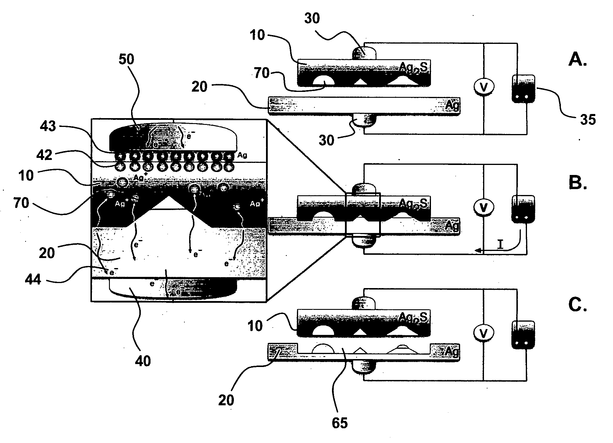
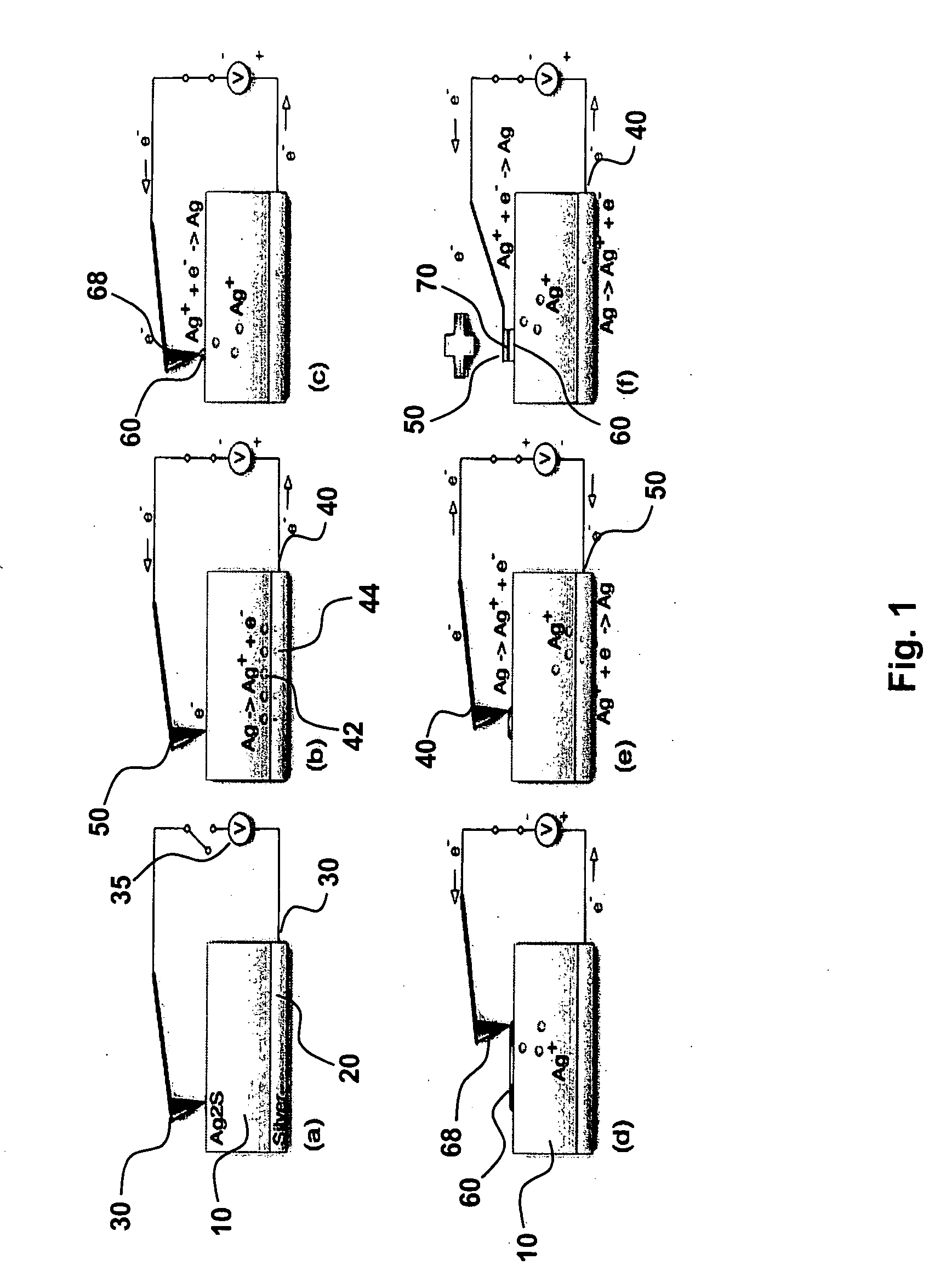
[0081] Reprogrammable and reconfigurable active nanostructures and processes influence the functional materials and devices to obtain enhanced energy conversion and chemical sensing. These experiments address outstanding issues in molecular-scale nanofabrication with superionic conduction by: (1) Addressing and explaining the underlying mechanisms of nanoscale charge, mass and energy transport, and reaction kinetics involved in nanostructure formation as a result of ionic conduction in solids; (2) Identifying the factors controlling growth rate and shape fidelity in the grown structures and exploiting this knowledge to develop a highly scalable and reprogrammable, in-parallel transfer stamping process; (3) Exploiting the new capability of programmable and reconfigurable patterning of nanostructures to actively regulate ionic transport and electron flow towards enhanced energy conversion and chemical s...
example 2
Direct Nanopatterning with Solid Ionic Stamping
[0100]FIG. 15A is an SEM image of an Ag2S solid state ionic conductor stamp used for electrochemical stamping and FIG. 15B an SEM image of the corresponding pattern etched in Ag metal.
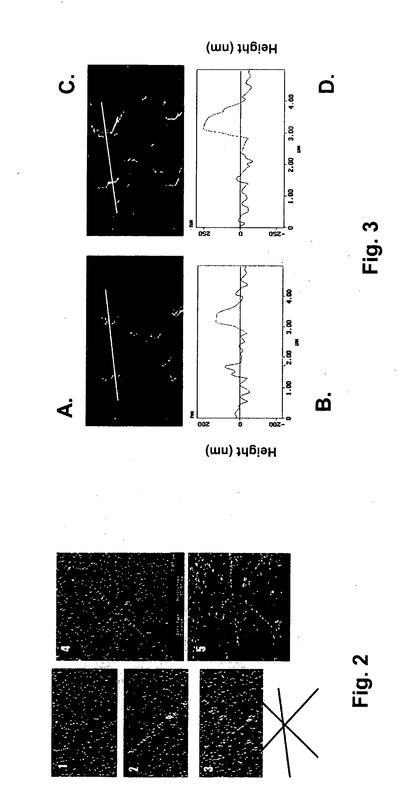
[0101] This example discloses an embodiment for generating sub-hundred nanometer features that integrates and extends the concepts of nanoimprint lithography and electrochemical micromachining. Realized by the mass transport property of solid-state ionic conductors and their dimensional integrity, this technique provides simplicity and high throughput of single-step pattern generation while keeping high feature resolution and reproducibility. In an embodiment, the solid-state ionic conductor is silver sulfide and is made into a stamping tool on which calibration features are defined to verify the lateral resolution capabilities of this technique. Stamping is achieved under various driving potentials and sub-hundred-nanometer lateral resolution is obtaine...
example 3
Electrochemical Stamping
[0123] The invention disclosed herein provides a unique and new capability to pattern metals with sub-100 nm resolution in a high-through put stamping process. For example, FIG. 22 shows arrays of patterns can be etched in metal. Depending on manufacturing considerations, such a 5×5 array may be created using single step electrochemical stamping, or alternatively, the metal may be repeatedly stamped to obtain the array. FIG. 23 shows the stamps of the present invention provide structures having sub-100 nm resolution. For example, multiple distinct lines or channels are generated that are separated by 50 nm and the lateral resolution is 60 nm. In an embodiment, the process is a solid-state, room temperature process that is highly compatible with a large variety of process technologies. Although the examples provided herein utilize silver, different ionic crystals for other materials, including but not limited to copper, and gold, can be similarly used, to obt...
PUM
| Property | Measurement | Unit |
|---|---|---|
| Thickness | aaaaa | aaaaa |
| Thickness | aaaaa | aaaaa |
| Pressure | aaaaa | aaaaa |
Abstract
Description
Claims
Application Information