
Method for Forming Zno Nano-Array and Zno Nanowall for Uv Laser On Silicon Substrate

a technology of uv laser and nano-array, which is applied in the direction of semiconductor lasers, crystal growth processes, polycrystalline material growth, etc., can solve the problems of high vacuum condition, inability to form a large-area zno nano-array, and inability to form large-area zno nano-array arrays. , to achieve the effect of excellent laser characteristics and superior laser characteristics

Inactive Publication Date: 2007-09-27
NANOHYBRID CO LTD
View PDF6 Cites 16 Cited by
  • Summary
  • Abstract
  • Description
  • Claims
  • Application Information

AI Technical Summary

Benefits of technology

"The present invention provides a method for forming a high-quality ZnO nanorod array on a substrate with controlled orientation and size. The method involves coating the substrate with uniform ZnO nanoparticles that serve as both a buffer layer and a seed layer, and growing the nanoparticles into crystals in a nutrient solution containing specific ions. The resulting nanorod array exhibits superior laser characteristics and is easily produced at low temperatures. Additionally, the invention provides a method for forming a new morphology of ZnO nanowalls with controlled size and thickness. The nanowalls have superior laser characteristics and are easier to induce than other nanorod arrays."

Problems solved by technology

However, the above technologies generally require expensive equipment, high vacuum condition, high-temperature heat treatment, and the like.
In particular, due to the difficulty of fabrication of vacuum chambers that can sustain high vacuum, it is impossible to form a large-area ZnO nanorod array.
Furthermore, high-temperature heat treatment causes numerous oxygen defects.
These oxygen defects are a major cause of broad green emission at about 510 nm and increase the laser threshold by interfering with UV emission.
Even though no expensive equipment is used for this method, there is a limitation on the type of a substrate that can be used for such a high-temperature heat treatment.
However, these substrates are very costly, which renders industrial application difficult.
However, there are disadvantages with Si-wafer are that a lattice mismatch with ZnO is very high (about 40%), and amorphous SiO2 rapidly grows at a low temperature, relative to ZnO, thereby preventing the crystal growth of ZnO [Appl. Phys. Lett., 78, 1511, 2001].
However, there arise other problems such as random growth of ZnO on a Si-wafer from a nutrient solution in a hydrothermal synthesis condition, imperfect orientation of ZnO rods due to very large lattice mismatch between the Si-wafer and ZnO, and formation of ZnO microrods [Chem. Comm., 80, 2002., Adv. Mater., 14, 1221, 2002, and J. Phys. Chem. B, 105, 3350, 2001].

Method used


Image

  • Method for Forming Zno Nano-Array and Zno Nanowall for Uv Laser On Silicon Substrate
  • Method for Forming Zno Nano-Array and Zno Nanowall for Uv Laser On Silicon Substrate
  • Method for Forming Zno Nano-Array and Zno Nanowall for Uv Laser On Silicon Substrate

Examples


example 1

[0041] ZnO nanoparticles were synthesized by (1) synthesizing precursors from Zn acetate and ethanol (99.5%) followed by (2) hydrolysis with LiOH. In more detail, a solution of 0.01 M Zn acetate in 100 ml ethanol was placed in a 250 ml Erlenmeyer flask equipped with a reflux condenser. The reaction solution was refluxed and distilled at 78 to 85° C. for about 3 hours until the volume of the reaction solution reduced to 40 ml. In this step, a reaction time is very important. If the reaction time exceeds 3 hours, bulky nonuniform particles may be created, whereby the solution becomes turbid. On the other hand, if it is less than 3 hours, functions as precursors may be lowered. Final product of precursors must be clear and transparent. 40 ml of precursors solution obtained were diluted with 60 ml of 0.1 M LiOH ethanol solution. At this time, if the temperature of the reaction solution is increased, the crystal size of ZnO may increase, thereby producing a suspension. To solve this prob...

example 2

[0043] A Si-wafer to be used in the present invention was pretreated as follows. First, the Si-wafer was washed with acetone in an ultrasonic bath and then subjected to removal of organic substances using a piranha solution (a mixed solution composed of 30% H2SO4 and H2O2 in a 2:1 volume ratio) at room temperature for about 30 minutes. Amorphous SiO2 on the Si-wafer was also removed using a 20% HF solution. The Si-wafer thus obtained was temporarily free from Si oxidation due to hydrogen coated on surface oxygen.

[0044] The Si-wafer after pretreatment was dip-coated with the ZnO nanoparticles synthesized in Example 1 at a rate of 4.21 cm / min and thermally treated at about 200° C. to immobilize the ZnO nanoparticles on the Si-wafer. However, a final product is not affected even when the thermal treatment is omitted.

example 3

[0045] A nutrient solution for formation of a ZnO nanorod array was prepared by mixing a 0.1M Zn nitrate solution and a 0.1M hexamethylenetetramine (HMTA) solution in a volume ratio of 1 to 1 (pH=about 7.0). The ZnO nanoparticles-dip coated Si-wafer prepared in Example 2 was placed in a Teflon autoclave and then incubated with the nutrient solution at 95° C. for about 6 hours. However, a nanorod array can be formed even when the thermal treatment was performed for less than 1 hour. The final product was washed with deionized water (18.2 μΩ) followed by water removal at about 100° C.

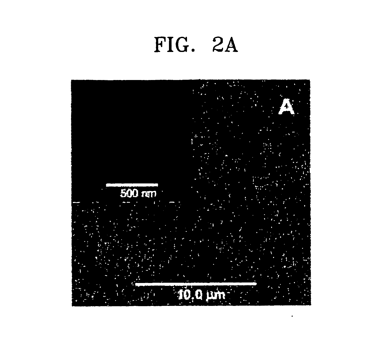
[0046]FIG. 2 is Scanning Electron Microscopy (SEM) images of surface(FIG. 2A), and a cross-section(FIG. 2B), and a TEM image of cross-section (FIG. 2C) of the ZnO nanorod array formed on the Si-wafer. As shown in FIG. 2, very dense ZnO nanorods of about 100 nm in diameter and about 1.5 μm in length were perfectly oriented on the Si-wafer.

[0047]FIG. 3 is a powder X-ray diffraction pattern of the ZnO nano...


PUM

PropertyMeasurementUnit
temperatureaaaaaaaaaa
lengthaaaaaaaaaa

Abstract

Provided are low-temperature formation methods of a perfectly oriented ZnO nanorod array and a new-type ZnO nanowall array having a new crystal growth rate, morphology, and orientation, from ZnO nanoparticles coated on a substrate. The method of forming the ZnO nanorod array includes synthesizing ZnO nanoparticles, coating on a substrate the ZnO nanoparticles serving both as a buffer layer and a seed layer, and growing the ZnO nanoparticles into crystals in a nutrient solution containing Zn nitrate, Zn acetate, or a derivative thereof, and hexamethylenetetramine. The method of forming the ZnO nanowall array includes synthesizing ZnO nanoparticles, coating on a substrate the ZnO nanoparticles serving both as a buffer layer and a seed layer, and growing the ZnO nanoparticles into crystals in a nutrient solution containing Zn acetate or its derivative and sodium citrate.

Description

TECHNICAL FIELD [0001] The present invention relates to low-temperature formation methods of a perfectly oriented and grown ZnO nanorod array and a new type ZnO nanowall array having new crystal growth rate, morphology, and orientation, on a ZnO nanoparticle-coated substrate. BACKGROUND ART [0002] Recently, there has been observed room-temperature UV laser emission in ZnO semiconductors. Therefore, much attention has been paid to ZnO semiconductors as promising substitutes for Group III-V nitride semiconductors that have been most widely used for UV-lasers and light-emitting diodes (LEDs). With respect to bulk ZnO, laser emission is observed only at an ultra-low temperature. However, as the size of ZnO is reduced to a nanometer level, room-temperature laser emission occurs. In this respect, numerous studies that have been made hitherto have been focused on enhancement of laser characteristics by size-reduction of ZnO. [0003] Generally, in UV laser of ZnO, the [0001] polar planes pla...

Claims


Application Information

Patent Timeline
Patent Type & Authority Applications(United States)
IPC IPC(8): B82B3/00H01S5/02H01S5/34H01S5/347
CPCB82Y20/00B82Y30/00C30B7/10H01S5/347C30B29/62H01S5/021H01S5/341C30B29/16B82B3/00B82Y40/00
Inventor CHOY, JIN HOJANG, EUE SOONWON, JUNG HEE
Owner NANOHYBRID CO LTD
Learn More