
Optical communication device and quantum key distribution system using the same

a communication device and quantum key technology, applied in the field of optical communication systems, can solve the problems of deterioration in waveform, difference in propagation delay, and difficulty in achieving higher speed only by using ask, so as to reduce optical loss, reduce the intensity of transmitted optical pulses, and achieve higher speed

Inactive Publication Date: 2007-10-25
NEC CORP
View PDF7 Cites 28 Cited by
  • Summary
  • Abstract
  • Description
  • Claims
  • Application Information

AI Technical Summary

Benefits of technology

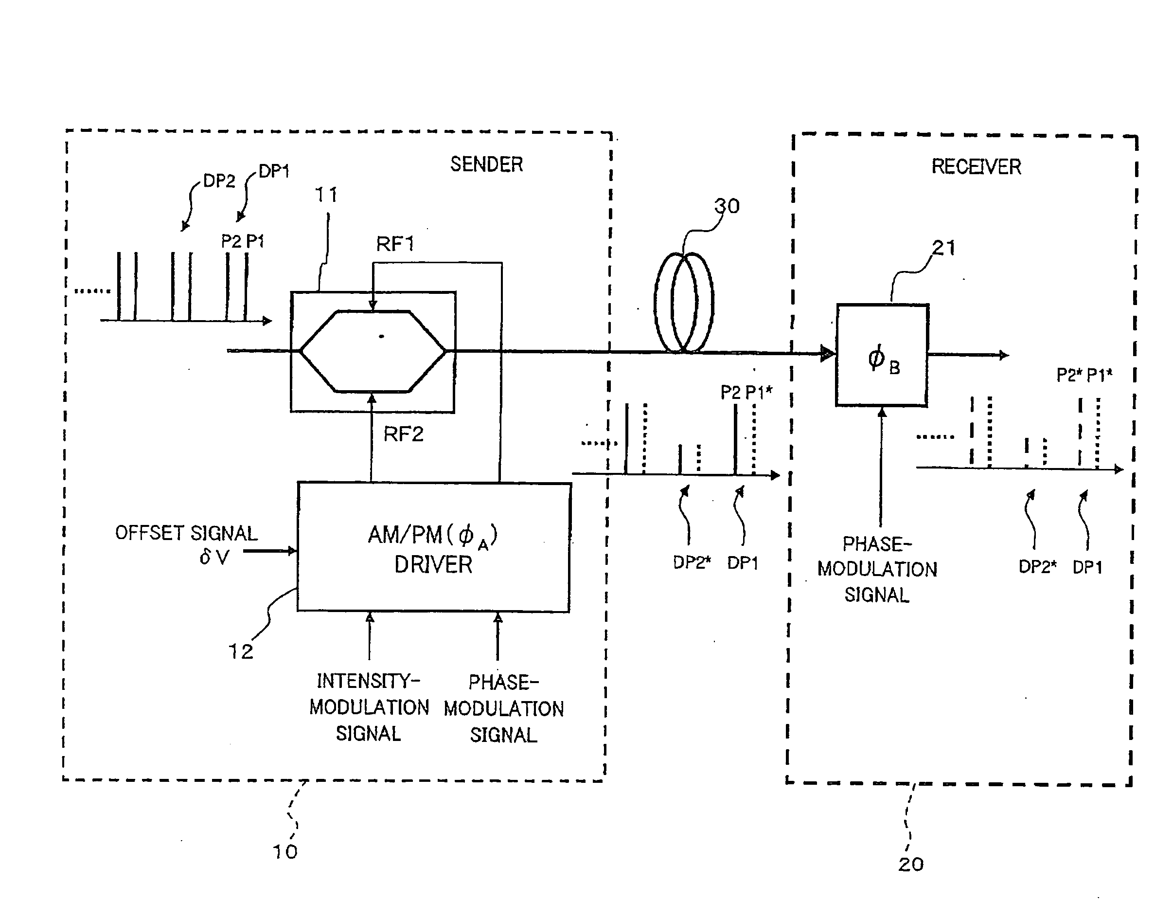
[0025]Accordingly, an object of the present invention is to provide an optical communication apparatus and a quantum key distribution system that can perform stable intensity and phase modulation on an optical pulse at high speed.
[0026]Another object of the present invention is to provide an optical communication apparatus and a quantum key distribution system that can enhance the cryptographic key generation rate.
[0030]In the case of the loop-back section including a polarization beam splitter loop, the optical modulator is preferably provided on an optical path of the loop-back section. Since the optical pulse is returned through the polarization beam splitter and the optical modulator, the optical loss can be reduced.
[0031]In a preferable embodiment of the present invention, the optical modulator is a dual-electrode Mach-Zehnder modulator. More specifically, the driver includes: a first digital-to-analog converter for generating a first modulation signal from binary phase-modulation information inputted as MSB (Most Significant Bit) and inverted one of binary intensity modulation information inputted as LSB (Least Significant Bit); a second digital-to-analog converter for generating a second modulation signal from the binary phase-modulation information inputted as MSB (Most Significant Bit) and the binary intensity modulation information inputted as LSB (Least Significant Bit); a first amplifier for amplifying the first modulation signal; a second amplifier for amplifying the second modulation signal; and an adder for adding a predetermined offset signal to an output signal of the second amplifier. In this case, an output signal of the first amplifier is applied as a first driving signal to one electrode of the dual-electrode Mach-Zehnder modulator and an output signal of the adder is applied as a second driving signal to the other electrode of the dual-electrode Mach-Zehnder modulator. The first and second amplifiers preferably amplify the first and second modulation signals respectively so that a voltage difference between adjacent levels of the output signals of the first and second amplifiers becomes equal to a level that is half a driving voltage Vπ of the dual-electrode Mach-Zehnder modulator. specifically, the predetermined offset signal allows the output signal of the second amplifier to deviate from half the driving voltage Vπ by a predetermined voltage.
[0034]As described above, phase modulation and intensity modulation can be concurrently performed by driving a single optical modulator according to modulation information. Accordingly, a smaller number of optics components can be used, resulting in reduced optical loss due to the optics through which an transmission optical pulse is transmitted. Accordingly, deterioration in the intensity of a transmitted optical pulse can be effectively suppressed. Specifically, when a Mach-Zehnder modulator is used as the optical modulator, it operates at much higher speed and the phase change can be also set more accurately, compared to a variable optical attenuator, resulting in stable intensity and phase modulation on an optical pulse at high speed.
[0035]In the case where the present invention is applied to a decoy QKD system in which the mean number of photons is varied, phase modulation and intensity modulation can be concurrently performed by driving a single optical modulator, allowing the timing design to be greatly simplified and the cryptographic key generation rate to be significantly enhanced. In addition, since a small number of optics components through which a transmission optical pulse is transmitted can be used, the cryptographic key generation rate due to the operable band of optics in use can be dramatically improved.

Problems solved by technology

In the present circumstances where the rapid growth in internet traffic continues, one of the most significant challenges is to enhance transmission bandwidth or transmission speed.
However, since around the time the data transmission speed per carrier exceeded 10 Gb / s, it has been difficult to accomplish higher speed only by using ASK.
One of the reasons for this is deterioration in waveform due to wavelength dispersion, which is typical of optical transmission lines.
This accumulated dispersion after propagation results in a difference in propagation delay, that is, causes waveform distortion.
Therefore, if an attempt is made to obtain the same code error rate as that achieved by a binary modulation scheme such as ASK or BPSK, a large carrier-to-noise ratio (CNR) is needed.
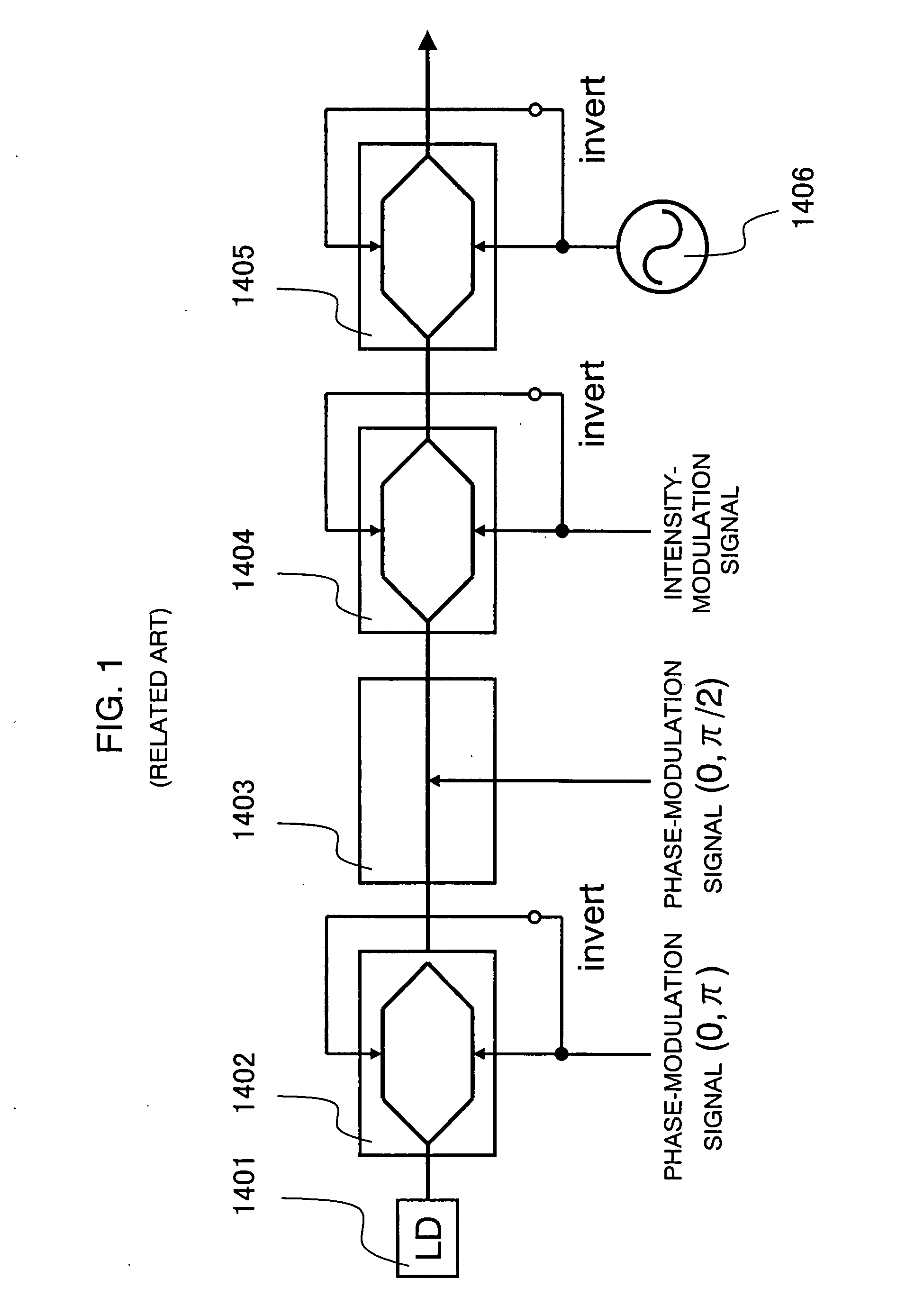
However, the use of modulators at multiple stages in generating an APSK signal, as in the transmitter of S. Hayase et al., increases loss and therefore reduces the intensity of output light, that is, the power of carrier.
Here, although the intensity of transmitted light can be set high by using an optical amplifier, it is impossible to avoid degradation of the signal-to-nose ratio (SNR) at the time of signal transmission.
However, according to the Heisenberg's uncertainty principle, it is impossible to perfectly return a once-observed photon to the quantum state before observation.
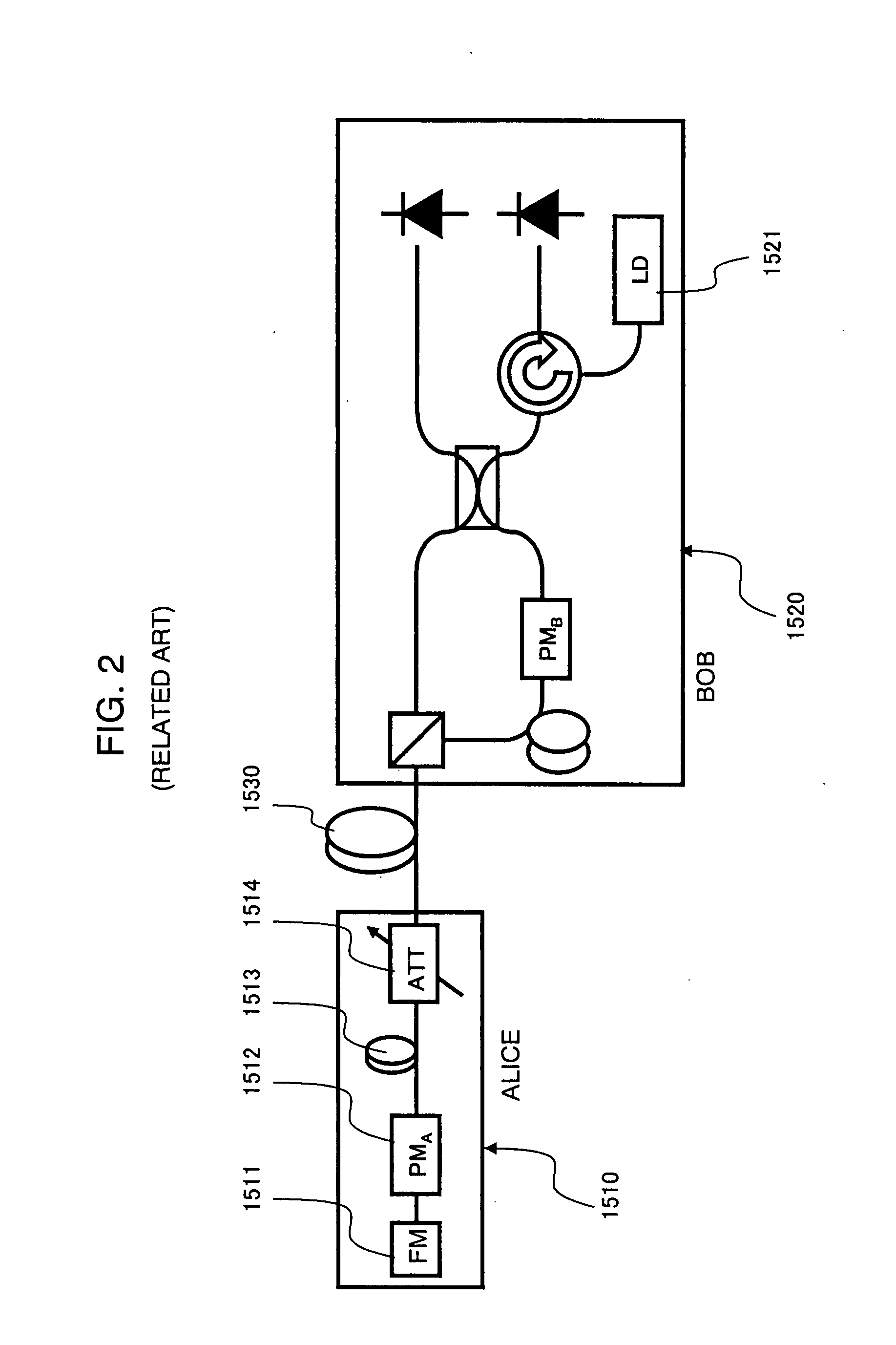
However, in the case of implementing QKD in the real world, for lack of useful single-photon light sources, an alternative method is used in which the light intensity of an optical pulse generated by a laser diode (LD) for general communication is lowered to a single-photon level (weak coherent state) by using an optical attenuator.
In such a decoy-state QKD system, however, a sender (Alice) in the conventional decoy-state QKD technology cannot perform both phase modulation and intensity modulation on each optical pulse at high speed with high reliability.
However, there are no variable optical attenuators that can operate at high speeds in the gigahertz range or so while ensuring the amount of attenuation for each of the polarization axes with accuracy.
Therefore, the operable optical pulse repetition rate has a limit, resulting in a limit being imposed on the cryptographic key generation rate.
Additionally, in the two-way system described in Zhao et al., backscattered light of an optical pulse occurring on the outward journey (mainly due to Rayleigh scattering with non-changing wavelength) degrades the characteristics of the system as noise light.
However, since the signal light suffers optical loss inside the sender (Alice), the signal light might be lost in the backscattered noise light in an extreme case.
Therefore, the optical loss inside the sender is large.
Therefore, a timing design is difficult to make, and there arises a limit to the QKD system driving rate.

Method used


Image

  • Optical communication device and quantum key distribution system using the same
  • Optical communication device and quantum key distribution system using the same
  • Optical communication device and quantum key distribution system using the same

Examples


first embodiment

2. First Embodiment

[0092]2.1) System Configuration

[0093]FIG. 9 is a block diagram showing a configuration of a two-way quantum key distribution (QKD) system according to a first embodiment of the present invention. Here, it is assumed that a sender (Alice) 40 and a receiver (Bob) 50 are connected through an optical fiber transmission line 60.

[0094]First, an optical pulse outputted from a laser light source 501 in the receiver 50 is sent to an optical coupler 503 by a circulator 502 and split into two pulses by the optical coupler 503. One of the two optical pulses is directly sent to a polarization beam splitter 505, allowed to pass through it, and then sent out to the transmission line 60. The other optical pulse is allowed through a phase modulator 504, sent to the polarization beam splitter 505, reflected there, and then sent out to the transmission line 60. The two optical pulses can be made to arrive at the polarization beam splitter 505 at different times by giving a differenc...

second embodiment

3. Second Embodiment

[0120]The present invention can be applied not only to two-way quantum key distribution systems but also to one-way systems.

[0121]FIG. 15 is a block diagram showing a schematic configuration of a one-way QKD system according to a second embodiment of the present invention. The present embodiment is a one-way QKD system using the planar lightwave circuit (PLC) described in Nambu, Y., et al., “One-way Quantum Key Distribution System based on Planar Lightwave Circuits,” quant-ph / 0603041, to which the present invention is applied. A sender or transmitter (Alice) 70 and a receiver (Bob) 80 are connected through optical fiber 90 and each have an interferometer for time-delayed pulses, structured by using an asymmetric Mach-Zehnder interferometer (AMZI) based on PLC technology.

[0122]The sender 70 has a pulse light source 701, an asymmetric Mach-Zehnder interferometer 702 based on a planar lightwave circuit, a MZ modulator 703 capable of intensity modulation and phase mo...


PUM

PropertyMeasurementUnit
voltageaaaaaaaaaa
voltageaaaaaaaaaa
voltageaaaaaaaaaa

Abstract

An optical communication apparatus that can perform stable intensity and phase modulation on an optical pulse at high speed is provided, as well as a quantum key distribution system using the apparatus. Using multilevel signals for the electric signals (RF1, RF2) to be applied to two arms of a two-electrode Mach-Zehnder modulator, phase modulation is performed on an optical pulse in accordance with the average of the levels of the signals (RF1, RF2), and intensity modulation is performed on the optical pulse in accordance with the voltage difference between the signals (RF1, RF2), whereby stable high-speed multilevel modulation can be realized. The cryptographic key generation rate in a decoy quantum key distribution system is enhanced.

Description

BACKGROUND OF THE INVENTION[0001]1. Field of the Invention[0002]The present invention relates to an optical communications system and, more particularly, to an optical communication apparatus that modulates the intensity and phase of an optical signal to be transmitted, as well as to a quantum key distribution system using the optical communication apparatus.[0003]2. Description of the Related Art[0004]In the present circumstances where the rapid growth in internet traffic continues, one of the most significant challenges is to enhance transmission bandwidth or transmission speed. This is no exceptional matter with trunk optical networks. Various research institutes and laboratories are working toward an increase in the data transmission speed per carrier in order to expand transmission capacities by utilizing the existing infrastructures without adding transmission lines and repeaters. Data transmission speeds continue to increase also in practical commercial transmission systems.[...

Claims


Application Information

Patent Timeline
Patent Type & Authority Applications(United States)
IPC IPC(8): H04B10/04G02F1/03G02F1/035H04B10/07H04B10/516H04B10/524H04B10/54H04B10/556H04B10/58H04B10/61H04B10/70H04L9/08H04L9/12
CPCH04B10/505H04B10/5051H04L9/0858H04B10/548H04B10/70H04B10/54
Inventor TANAKA, AKIHIROTAJIMA, AKIOTAKAHASHI, SEIGOMAEDA, WAKAKO
Owner NEC CORP
Learn More