Wavelength conversion chip for use with light emitting diodes and method for making same

Inactive Publication Date: 2008-02-21
GOLDENEYE
View PDF7 Cites 110 Cited by
  • Summary
  • Abstract
  • Description
  • Claims
  • Application Information

AI Technical Summary

Benefits of technology

[0023] Because the fabrication of the wavelength conversion chip is independent of the LED fabrication, processes such as annealing, thermal and electron beam aging, recrystallization, and other processes known in the art can enhance the conversion efficiency of the wavelength conversion material or, in the case of phosphor powders, sinter the phosphor powders into ceramic elements either while the material is on the growth substrate or before application of the wavelength conversion chip to the LED. The resulting wavelength conversion chip can be homogeneous

Problems solved by technology

Though relatively inexpensive, the phosphors generated using this method suffer from high levels of dislocations and lattice defects.
In addition, the compositional purity is also difficult to maintain.
It has been shown, however, in accelerated aging studies that very high excitation levels can degrade the output luminescence of powdered phosphors severely and impact overall life performance.
Several material characteristics contribute to this degradation and/or loss in efficiency problem such as lattice defects, out-gassing, and compositional purity.
In the case of powdered phosphors, this can be a major issue because the phosphor particles are usually isolated from any reasonable thermal conduction path.
At very high excitation levels the energy associated with less than unity quantum efficiency and Stokes shift losses can induce a significant localized thermal rise within the phosphor particles.
The scattering created by the use of a powder can reduce the overall light output due to the backscattering and subsequent absorption of the generated light.
However, as-deposited thin film phosphors have relatively poor wavelength conversion efficiency.
This annealing step can damage the semiconductor layers of the LED.
In addition, the absorption cross-sections of most thin film phosphors are low, especially for blue and near ultraviolet (UV) excitations

Method used


Image

  • Wavelength conversion chip for use with light emitting diodes and method for making same
  • Wavelength conversion chip for use with light emitting diodes and method for making same
  • Wavelength conversion chip for use with light emitting diodes and method for making same

Examples


Embodiment Construction

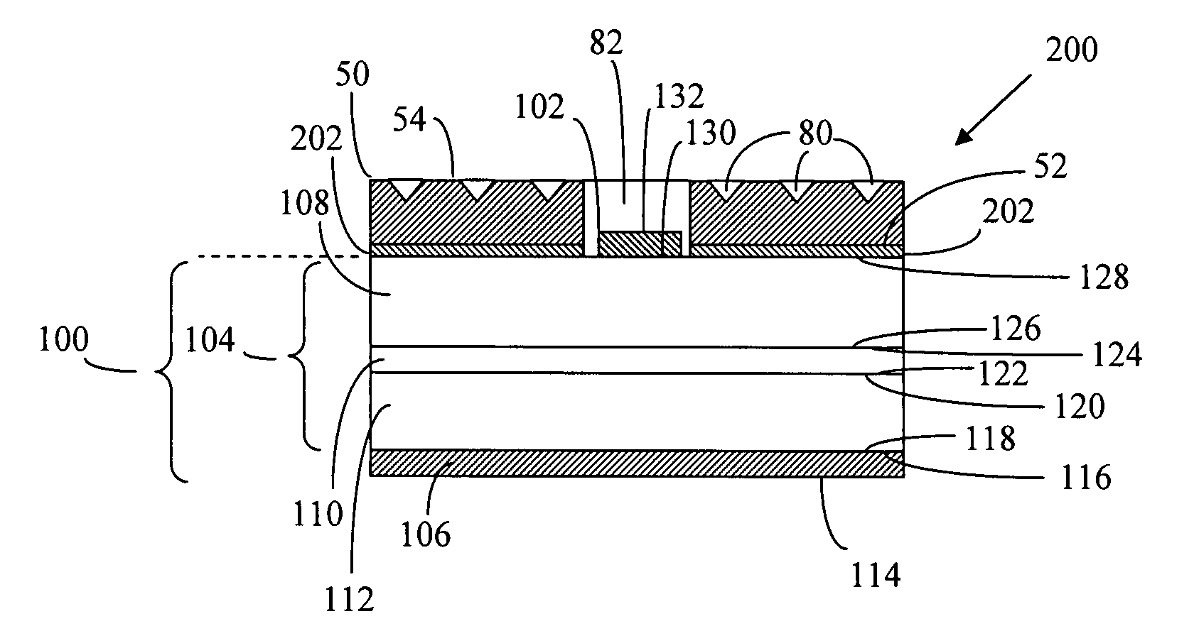
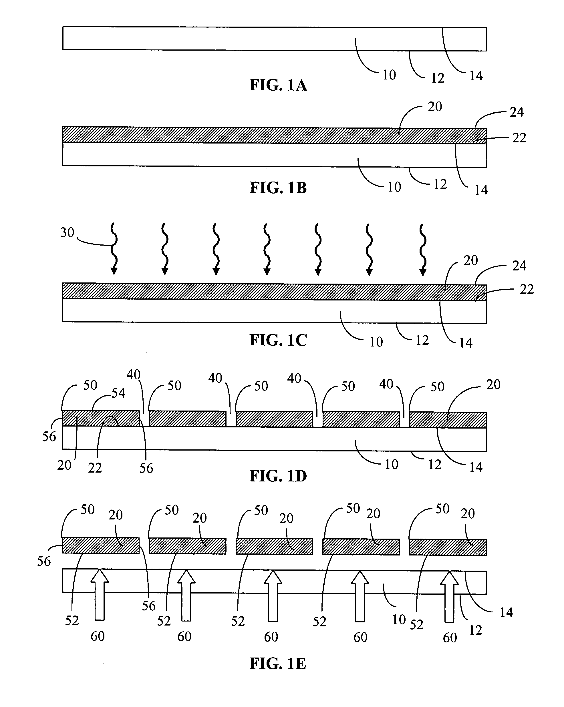
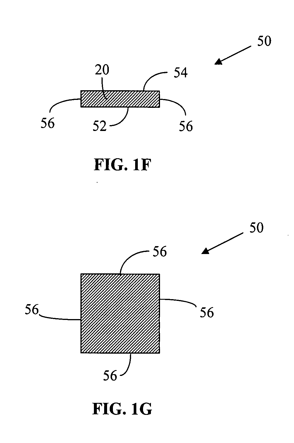
[0060] The preferred embodiments of the present invention will be better understood by those skilled in the art by reference to the above listed figures. The preferred embodiments of this invention illustrated in the figures are not intended to be exhaustive or to limit the invention to the precise form disclosed. The figures are chosen to describe or to best explain the principles of the invention and its applicable and practical use to thereby enable others skilled in the art to best utilize the invention. The above listed figures are not drawn to scale. In particular, the thickness dimensions of the LEDs and wavelength conversion chips are expanded to better illustrate the various internal layers of the devices.

[0061] An important solid-state light source is a blue or ultraviolet emitting LED used in conjunction with one or more wavelength conversion materials such as phosphors or quantum dots that convert at least some of the blue or ultraviolet light to other wavelengths. For ...


PUM


Abstract

A wavelength conversion chip is formed by depositing a wavelength conversion material on a substrate to form a layer, removing the resulting wavelength conversion layer from the substrate and then segmenting the wavelength conversion layer into a plurality of wavelength conversion chips. The wavelength conversion material can be annealed by thermal annealing or radiation annealing to increase the wavelength conversion efficiency of the chips or to sinter the wavelength conversion material to form a ceramic material. Optical coatings, vias, light extraction elements, electrical connections or electrical bond pads can be fabricated on the wavelength conversion chips.

Description

CROSS REFERENCE TO RELATED APPLICATIONS [0001] This application is a continuation-in-part of U.S. patent application Ser. No. 11 / 389,311 entitled “WAVELENGTH CONVERSION CHIP IN SOLID-STATE LIGHTING AND METHOD FOR MAKING SAME,” filed Mar. 24, 2006, and claims benefit therefrom.TECHNICAL FIELD [0002] A chip containing a wavelength conversion material and a method for making the chip. The chip can be used in conjunction with a light emitting diode (LED) to convert light emitted by the LED into another wavelength. BACKGROUND [0003] The recent proliferation of solid-state lighting has created a need for high performance wavelength conversion materials. The standard approach is to form wavelength conversion materials (e.g. phosphors) using solid state processing as known in the art. These phosphors are then ground down to powders in the micron size range and deposited on a surface using a variety of deposition techniques such as settling, encapsulation, and spray coating. Large extended a...

Claims


Application Information

Patent Timeline
IPC IPC(8): H01L33/00H01L21/78H01L33/50
CPCH01L33/508H01L2933/0041H05B33/10H01L2924/0002H01L2924/00
Inventor BEESON, KARL W.ZIMMERMAN, SCOTT M.LIVESAY, WILLIAM R.
Owner GOLDENEYE
Why Eureka
Try Eureka