Method for producing single crystal silicon solar cell and single crystal silicon solar cell

a technology of solar cells and solar cells, applied in the direction of final product manufacturing, sustainable manufacturing/processing, sustainable buildings, etc., can solve the problems of reducing affecting the efficiency of production, so as to achieve excellent crystallinity and improve conversion efficiency. , the effect of high conversion efficiency

Inactive Publication Date: 2008-05-01
SHIN ETSU CHEM IND CO LTD
View PDF29 Cites 40 Cited by
  • Summary
  • Abstract
  • Description
  • Claims
  • Application Information

AI Technical Summary

Benefits of technology

[0039]According to the method for producing a single crystal silicon solar cell of the present invention, it is possible to produce a see-through type thin-film solar cell which is excellent in crystallinity and has a single crystal silicon layer having a higher conversion efficiency as a light conversion layer.
[0040]Moreover, the single crystal silicon solar ce

Problems solved by technology

However, it is inappropriate to determine the effective utilization ratio of resources based on simple comparison with a film thickness required by a crystal-based solar cell, because of exemplary circumstances that high purity gas materials such as silane and disilane are used as starting materials for fabrication of amorphous silicon solar cells, and that the effective utilization ratio of the gas materials includes deposition thereof at locations in a plasma CVD apparatus other than at a substrate.
Further, an amorphous silicon solar cell has a conversion efficiency of about 10

Method used


Image

  • Method for producing single crystal silicon solar cell and single crystal silicon solar cell
  • Method for producing single crystal silicon solar cell and single crystal silicon solar cell

Examples


example

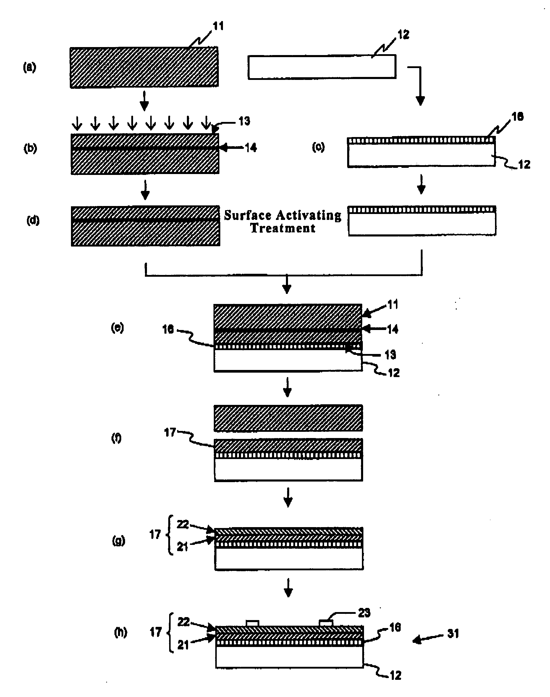
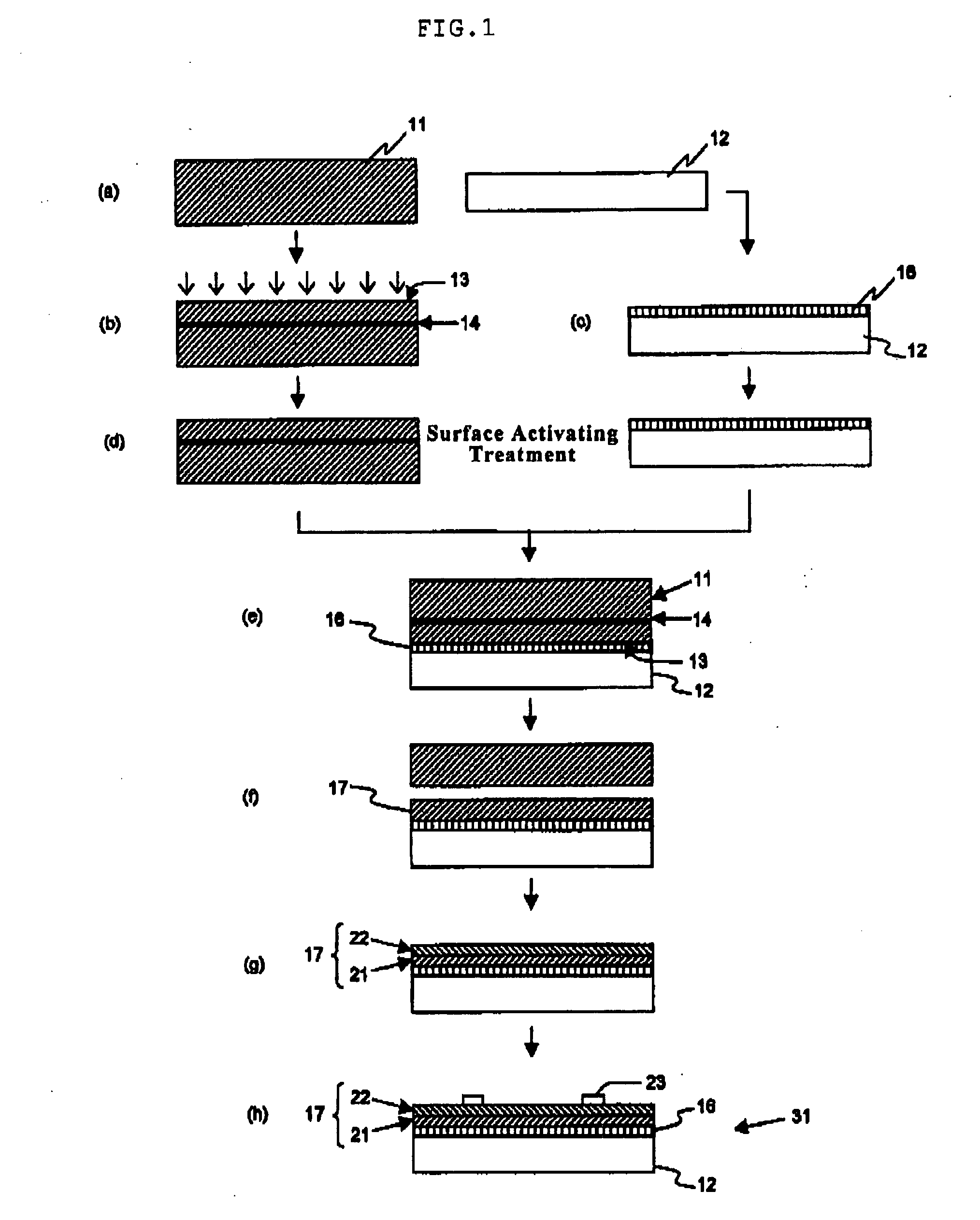
[0079]Prepared as a single crystal silicon substrate 11 was a single crystal silicon substrate of a p-type, having a diameter of 200 mm (8 inches), one surface which was mirror-polished, a crystal face (100), and a specific resistance of 15 Ω·cm. Further prepared as a transparent insulator substrate 12 was a quartz glass substrate having a diameter of 200 mm (8 inches) and a thickness of 2.5 mm (stage “a”).

[0080]Next, hydrogen cations were implanted into the single crystal silicon substrate 11 under a condition of an acceleration voltage of 350 keV and a dosage of 1.0×10¹⁷ / cm2 (stage “b”). This resulted in a depth of an ion implanted layer 14 at about 3 μm from an ion implanting surface 13.

[0081]Meanwhile, there was formed a coating of tin oxide doped with fluorine at a thickness of about 0.5 μm on one surface of the quartz glass substrate 12 by chemical vapor deposition, thereby providing a transparent electroconductive film 16 (stage “c”). The surface of the transparent electrocon...


PUM

PropertyMeasurementUnit
Depthaaaaaaaaaa
Depthaaaaaaaaaa
Electrical conductoraaaaaaaaaa

Abstract

There is disclosed a method for producing a single crystal silicon solar cell comprising the steps of: implanting hydrogen ions or rare gas ions into a single crystal silicon substrate through an ion implanting surface thereof to form an ion implanted layer in the single crystal silicon substrate; forming a transparent electroconductive film on a surface of a transparent insulator substrate; conducting a surface activating treatment for the ion implanting surface of the single crystal silicon substrate and/or a surface of the transparent electroconductive film on the transparent insulator substrate; bonding the ion implanting surface of the single crystal silicon substrate and the surface of the transparent electroconductive film on the transparent insulator substrate to each other; applying an impact to the ion implanted layer to mechanically delaminate the single crystal silicon substrate thereat to leave a single crystal silicon layer; and forming a p-n junction in the single crystal silicon layer. There can be provided a single crystal silicon solar cell where a light conversion layer is provided as a thin-film for effective utilization of silicon as a starting material of the silicon solar cell, which single crystal silicon solar cell is excellent in conversion characteristics and is less in degradation due to light irradiation, and which single crystal silicon solar cell is provided as a see-through type solar cell that is usable as a natural lighting window material of a house or the like.

Description

BACKGROUND OF THE INVENTION[0001]1. Field of the Invention[0002]The present invention relates to a method for producing a single crystal silicon solar cell and to a single crystal silicon solar cell, and particularly to a method for producing a single crystal silicon solar cell for forming a single crystal silicon layer on a transparent insulator substrate and to a single crystal silicon solar cell having a single crystal silicon layer over a transparent insulator substrate.[0003]2. Description of the Related Art[0004]Solar cells comprising silicon as main materials are classified into single crystal silicon solar cells, polycrystalline silicon solar cells, and amorphous silicon solar cells, based on crystallinities thereof. Among them, single crystal silicon solar cells are each provided as solar cell elements by cutting a single crystal ingot prepared by a crystal pulling method by a wire saw into a wafer shape slice, working the slice into a wafer having a thickness of 100 to 200...

Claims


Application Information

Patent Timeline
IPC IPC(8): H01L31/04B29C65/00H01L21/02H01L27/12H01L31/06H01L31/068H01L31/18
CPCH01L31/1804Y02E10/547Y02B10/10H01L31/1896Y02P70/50H01L31/04H01L31/06H01L31/18
Inventor ITO, ATSUOAKIYAMA, SHOJIKAWAI, MAKOTOTANAKA, KOICHITOBISAKA, YUUJIKUBOTA, YOSHIHIRO
Owner SHIN ETSU CHEM IND CO LTD
Why Eureka
Try Eureka