Semiconductor device and manufacturing method thereof

a semiconductor and semiconductor technology, applied in the direction of semiconductor devices, electrical devices, transistors, etc., can solve the problems of increasing the mounting cost of the silicon chip, the inability to reduce the unit cost of the wireless chip, and the inability to meet the requirements of the unit cost of the wireless chip, so as to reduce the variation of writing voltage among a plurality of memories and reduce the unit cost of the chip

Inactive Publication Date: 2008-09-18
SEMICON ENERGY LAB CO LTD
View PDF21 Cites 24 Cited by
  • Summary
  • Abstract
  • Description
  • Claims
  • Application Information

AI Technical Summary

Benefits of technology

[0046]A semiconductor device mounted with a memory which can be driven in the ranges of a current value and a voltage value which can be generated from a wireless signal can be realized, and also unit cost of a chip can be reduced. Further, variation of writing voltages among a plurality of memories can be reduced.

Problems solved by technology

Therefore, there has been an inevitable limit to reduce the unit cost of the wireless chips.
Further, reduction in cost can be expected by miniaturization of the silicon chip; however, mounting cost of the silicon chip is increased, when miniaturization of the silicon chip proceeds.
Since the wireless chip is attached to an article, there is a concern that a connection portion between the terminal of the silicon chip and the antenna may be disconnected due to thermal stress in view of being exposed under various environments.
Further, the conventional wireless chip is not suitable for being attached to a curved surface of an article even if the wireless chip is a smaller piece because it uses silicon for a structure.
In the case where a silicon chip has been mounted on a base formed of a flexible material, there has been a concern that a connection portion between the silicon chip and an antenna of the base might be destroyed when the base has been bent along the curved surface of the article.
Even if a wireless chip is thinned, in the case of an IC tag which is attached to an article to be used, disfigurement is caused because a protrusion occurs on a surface of the base when the wireless chip is attached to a thin base (for example, a strip of film or a slip of paper).
Further, since a protrusion occurs on the surface of the base, in the case of performing printing to a base such as a slip of paper, high-definition printing becomes difficult.
Furthermore, there has been a concern that, when a silicon chip is thinned, mechanical strength of the silicon chip might be decreased and the silicon chip might be broken when a base is bent.
Each silicon chip is minute, and a manufacturing device for supplying current for writing different data to a ROM which is formed in each silicon chip needs precision location alignment or the like, thereby being expensive.
Therefore, manufacturing cost is increased due to this manufacturing device.

Method used


Image

  • Semiconductor device and manufacturing method thereof
  • Semiconductor device and manufacturing method thereof
  • Semiconductor device and manufacturing method thereof

Examples


embodiment mode 1

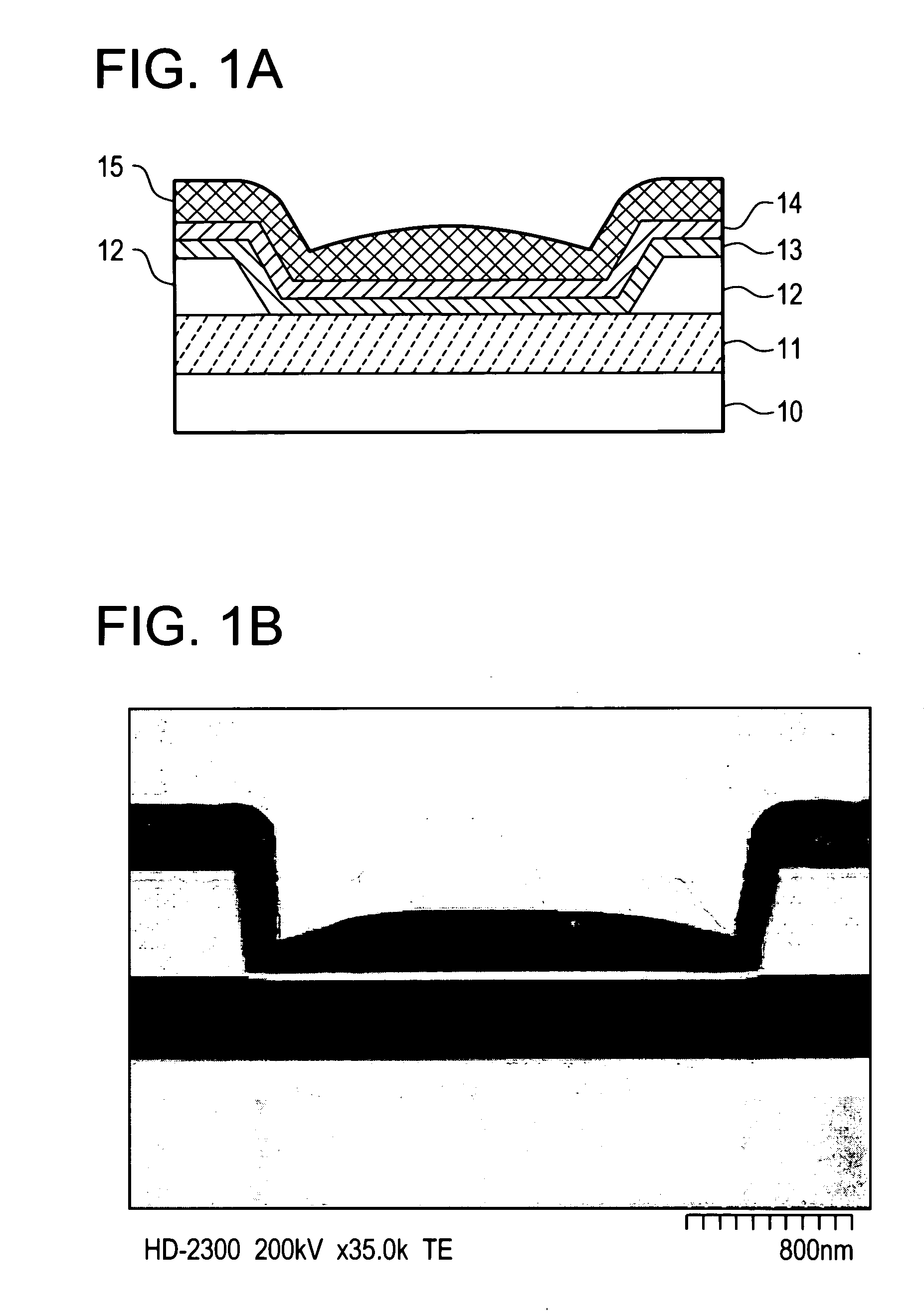
[0062]FIG. 1A shows a cross-sectional schematic view of an antifuse-type ROM of the present invention.

[0063]As an example is shown in FIG. 1A, the antifuse-type ROM of the present invention has a structure in which a first electrode 11 is formed over a substrate 10 having an insulating surface, and a silicon film 13, a germanium film 14, and a second electrode 15 are sequentially stacked over the first electrode 11.

[0064]These electrodes are short-circuited by voltage application between the first electrode 11 and the second electrode 15, whereby data is written to a memory element.

[0065]As materials of the first electrode 11 and the second electrode 15, a single substance of tungsten (W), titanium (Ti), nickel (Ni), chromium (Cr), molybdenum (Mo), tantalum (Ta), cobalt (Co), zirconium (Zr), vanadium (V), palladium (Pd), hafnium (Hf), platinum (Pt), iron (Fe), or the like, or an alloy or a compound thereof is used to form a conductive film by a sputtering method, which may be proces...

embodiment mode 2

[0080]A manufacturing process of a semiconductor device of the present invention will be described with reference to FIGS. 4A and 4B. A cross-sectional structure shown in FIG. 4A is a process diagram in the middle of manufacturing process of the semiconductor device.

[0081]First, a separation layer 102 and an insulating layer 103 are formed over a substrate 101 having an insulating surface. A quartz substrate, a glass substrate, or the like can be used as the substrate 101 having an insulating surface. In particular, a glass substrate which can have a large area of over 1 m on each side is suitable for mass production. A tungsten film having a thickness of 50 to 200 nm is used as the separation layer 102, and a silicon oxide film is used as the insulating layer 103. Note that the separation layer 102 is not limited to a tungsten film, and a tungsten nitride film, a molybdenum film, an amorphous silicon film, or the like may be used. In addition, the insulating layer 103 is not limite...

embodiment 1

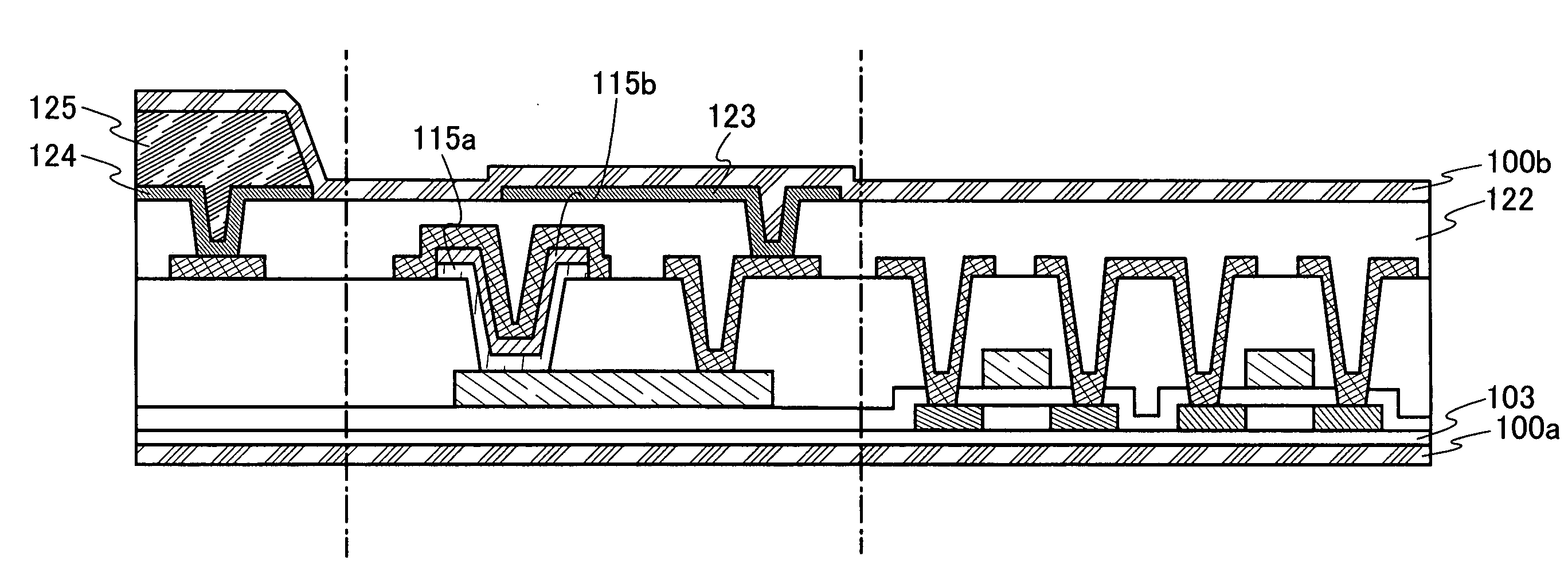
[0122]In this embodiment, a manufacturing method of a wireless chip including an active matrix antifuse-type ROM will be described below with reference to FIGS. 6A to 6D and FIGS. 7A to 7C.

[0123]First, a metal layer 502 which serves as a separation layer is formed over a substrate 501. A glass substrate is used as the substrate 501. A tungsten film, a tungsten nitride film, or a molybdenum film having a thickness of 30 to 200 nm which is obtained by a sputtering method is used for the metal layer 502.

[0124]Next, a surface of the metal layer 502 is oxidized to form a metal oxide layer (not shown). The metal oxide layer may be formed by oxidation of the surface with pure water or ozone water, or oxidation with oxygen plasma. Alternatively, the metal oxide layer may be formed by heating in an atmosphere containing oxygen. Further alternatively, the metal oxide layer may be formed in a later step of forming an insulating film. In this case, when a silicon oxide film or a silicon oxynitr...


PUM


Abstract

It is an object of the present invention to provide a semiconductor device mounted with a memory which can be driven in the ranges of a current value and a voltage value which can be generated from a wireless signal. It is another object to provide a write-once read-many memory into which data can be written anytime after manufacture of a semiconductor device. An antenna, an antifuse-type ROM, and a driver circuit are formed over a substrate having an insulating surface. A stacked layer of a silicon film and a germanium film is interposed between a pair of electrodes included in the antifuse-type ROM. The antifuse-type ROM having this stacked layer can reduce fluctuation in writing voltage.

Description

BACKGROUND OF THE INVENTION[0001]1. Field of the Invention[0002]The present invention relates to semiconductor devices each having a circuit including a thin film transistor (hereinafter referred to as a TFT) and manufacturing methods thereof. For example, the present invention relates to electronic appliances in each of which an electro-optical device typified by a liquid crystal display panel or a light-emitting display device including an organic light-emitting element is mounted as a component.[0003]Note that semiconductor devices in this specification refer to general devices which can function by utilization of semiconductor characteristics, and electro-optical devices, semiconductor circuits, and electronic appliances are all semiconductor devices.[0004]2. Description of the Related Art[0005]Various types of memories have conventionally been proposed. As typical memories, the following can be given: memories each including an electromagnetic tape or an electromagnetic disk, a...

Claims


Application Information

Patent Timeline
Patent Type & Authority Applications(United States)
IPC IPC(8): H01L29/786H01L21/336
CPCH01L27/13H01L27/1214H01L27/1266H01L27/1218H01L27/12H10B20/00
Inventor TOKUNAGA, HAJIMETAJIMA, RYOTA
Owner SEMICON ENERGY LAB CO LTD
Why Eureka
Try Eureka