
Interlayer of textured substrate for forming epitaxial film, and textured substrate for forming epitaxial film
- Summary
- Abstract
- Description
- Claims
- Application Information
AI Technical Summary
Benefits of technology
Problems solved by technology
Method used
Image

Examples
first embodiment
[0026]A copper tape plate having a {100} cube texture (Δφ≦6°), which had beforehand been subjected to orientation treatment, was prepared as a base material. Before the preparation of an interlayer, the surface of the copper plate was subjected to ion-beam etching for 20 minutes to remove matter adsorbed on the surface. Next, an interlayer consisted of an ITO film was formed on one surface of this base material. The formation of the ITO film was performed by the PLD method. By using an ITO (tin oxide content: 10 wt %) as a target, an ITO film having a film thickness of 350 nm was formed at a substrate temperature of 650° C., at a gas pressure of 3.8×10⁻² Pa, and with a laser frequency of 2.5 Hz. A textured substrate provided with an interlayer of a single ITO layer was fabricated by the above-described steps.
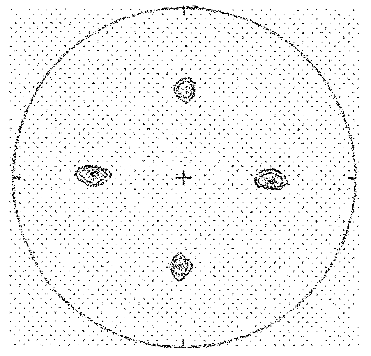
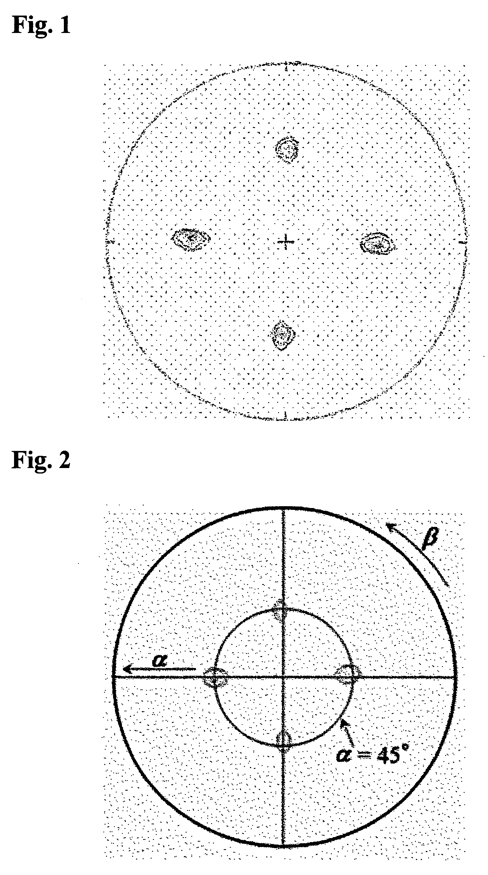
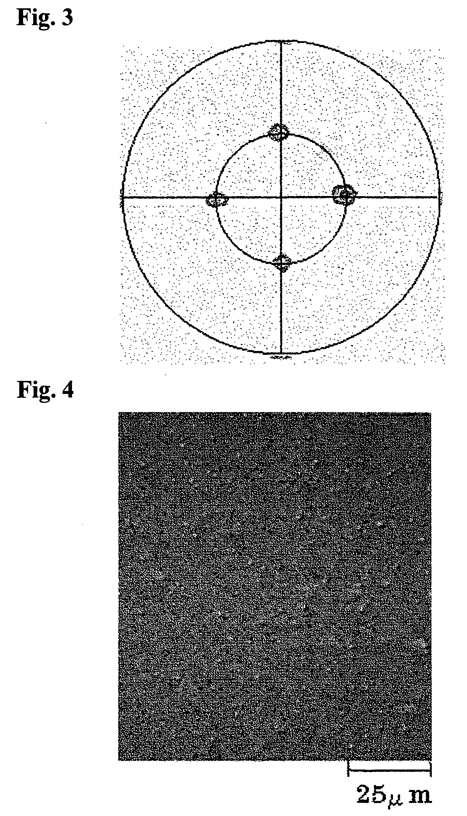
[0027]The surface of the fabricated textured substrate provided with an ITO layer was subjected to an X-ray pole figure analysis (XPFA). FIG. 1 is an ITO {111} pole figure obtai...
second embodiment
[0028]In this embodiment, a textured substrate provided with an interlayer of a multilayer structure with an ITO film as the bottom layer was fabricated by using the copper tape fabricated in the first embodiment as a base material, and a superconductor (YBCO) was formed thereon as an epitaxial film.
[0029]First, an ITO film was formed on a tape-like copper base material as used in the first embodiment under the same conditions as in the first embodiment. And upon the ITO film, a multilayer film of YSZ and the like was formed as follows. After that, a superconductor film was formed. The formation of the interlayer and the superconductor film was performed by the PLD method.
TABLE 1Manufacturing conditionsGasLatticeFilmSubstratepressureCompositionMaterialconstantthicknessTargettemperature(Pa)Base materialCu3.62 Å————InterlayerFirstITO10.12 Å 350 nmITO650° C.3.8 × 10−2layer(Ar)SecondYSZ5.15 Å100 nmYSZ750° C.3.8 × 10−2layer(Ar)ThirdCeO25.41 Å100 nmCeO2800° C.3.8 × 10−2layer(Ar)FourthSTO3...
third embodiment
[0033]In this embodiment, a textured substrate in which an interlayer of a multilayer structure with ITO as the bottom layer is formed on a nickel base material, was fabricated, and a superconductor (YBCO) was formed thereon as an epitaxial film.
[0034]An ITO film was formed under the same conditions as used in the first and second embodiments on a tape-like nickel tape material having a {100} cube texture (Δφ≦7°), which had been subjected to orientation treatment. And upon the ITO film, a superconductor film was formed by forming a cerium oxide film and the like as shown in Table 2. The formation of the interlayer and the superconductor film was performed by the PLD method.
TABLE 2Manufacturing conditionsGasLatticeFilmSubstratepressureCompositionMaterialconstantthicknessTargettemperature(Pa)Base materialNi3.52 Å————InterlayerFirstITO10.12 Å 350 nmITO650° C.3.8 × 10−2layer(Ar)SecondYSZ5.15 Å100 nmYSZ750° C.3.8 × 10−2layer(Ar)ThirdCeO25.41 Å100 nmCeO2800° C.3.8 × 10−2layer(Ar)Supercond...
PUM
| Property | Measurement | Unit |
|---|---|---|
| Thickness | aaaaa | aaaaa |
| Surface roughness | aaaaa | aaaaa |
Abstract
Description
Claims
Application Information