
Method of producing large area SiC substrates

Active Publication Date: 2009-01-15
NORTHROP GRUMMAN SYST CORP
View PDF6 Cites 14 Cited by
  • Summary
  • Abstract
  • Description
  • Claims
  • Application Information

AI Technical Summary

Problems solved by technology

Commonly used substrates for growing semiconductor materials, such as sapphire and Si, typically cause large defects in the semiconductor materials grown on these substrates, which in turn adversely affect the performance and reliability of the electronic device employing the semiconductor materials.
The poor quality of the epitaxially grown semiconductor crystals is generally due to the unavailability of a lattice matched and chemically matched substrate.
Since the thickness of the film is considerably smaller than that of the substrate, the difference in lattice constant between the film and the substrate causes generation of strain and defects in the film.
For example, when a crystal of a nitride semiconductor, such as gallium nitride (GaN), is grown on a starting substrate made of silicon (Si) or the like and then cooled to the ordinary temperature, a large number of dislocations and cracks occur in the nitride semiconductor layer because of stress caused by the difference in thermal expansion coefficient or lattice constant.
This causes deterioration of the film characteristic.
However, SiC wafers, especially large SiC wafers, are very expensive.

Method used


Image

  • Method of producing large area SiC substrates
  • Method of producing large area SiC substrates
  • Method of producing large area SiC substrates

Examples


example 1

Deposition of SiC Films on Si Substrate Using RF Plasma with Resistive Heating of the Si Substrate

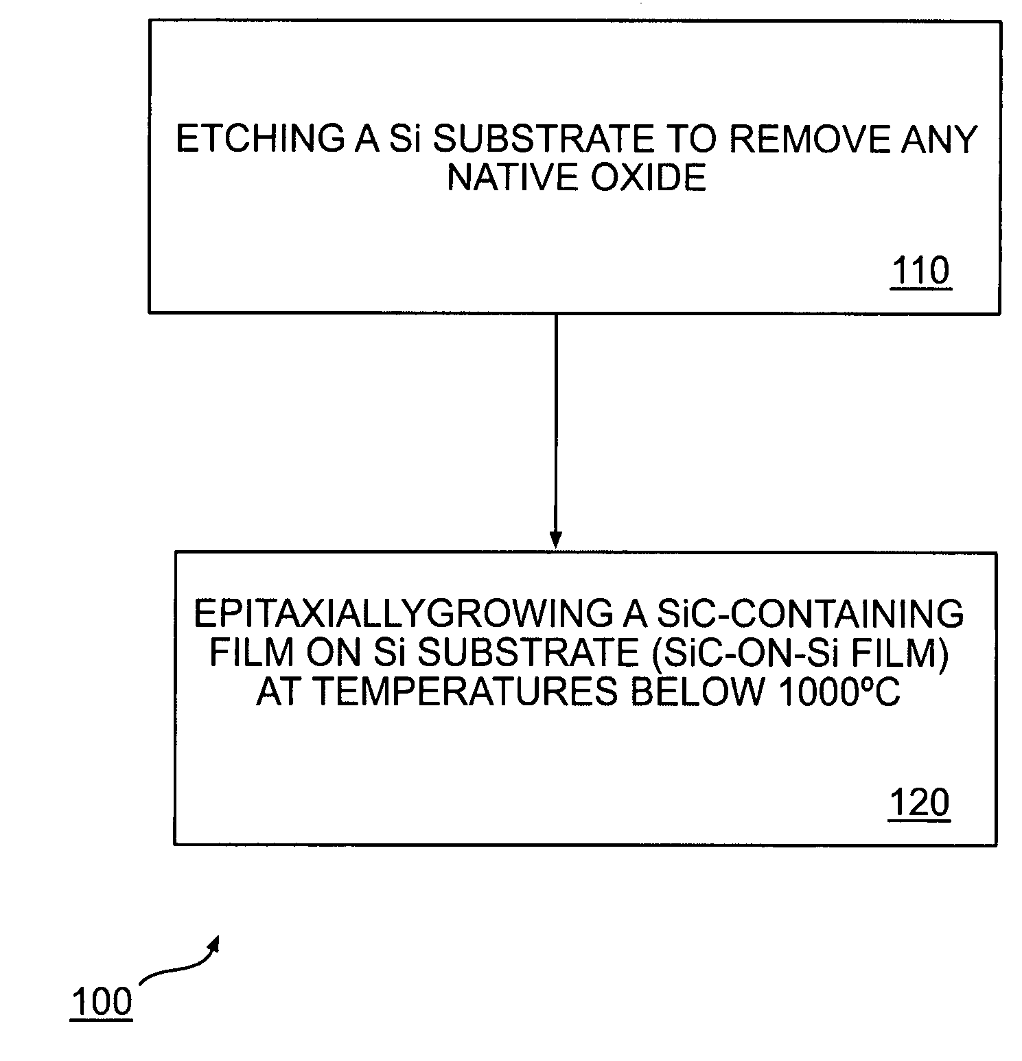
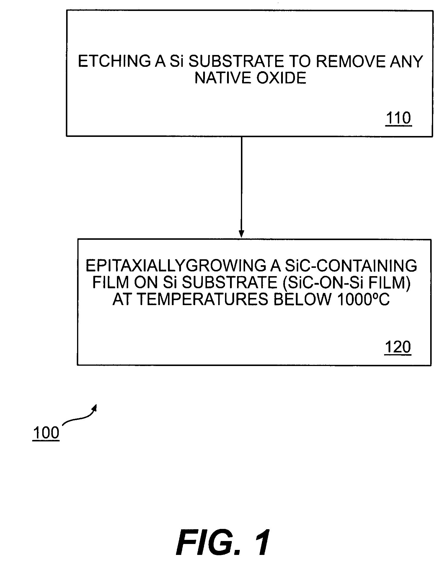
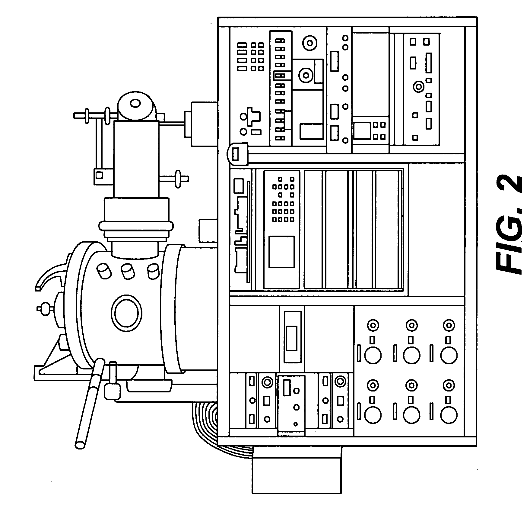
[0044]Two-inch, single-side polished Si (111) wafers were used as substrates. The Si wafers were etched in 10% HF to remove any native oxide. The etched wafer was dried with nitrogen gas and immediately loaded into the growth chamber of a sputtering system shown in FIG. 2.

[0045]Briefly, the Si substrate was clamped into a 2″ resistive heater and the chamber was evacuated to a base pressure of about 5×10⁻⁸ Torr. Once the base pressure was reached, the substrate / heater assembly was ramped to a 850° C. growth temperature at a ramp rate of 3° C. / minute. Argon gas was used as the RF plasma gas. The argon gas flow was set to 50 sccm. During deposition, the chamber was actively pumped and maintained a chamber pressure of about 8 mTorr. The RF forward power was 100 watts, with a DC bias of approximately −250V. The sputter gun used a 3″ SiC target.

[0046]The RF sputtered SiC on the Si substrate a...

example 2

Diode Devices Using SiC Film Deposited on Si Substrate

[0047]Several diode devices were created by lithographic patterning and evaporation of Cr / Au contacts to the SiC-on-Si film produced in Example 1. The processes used to create the devices (i.e., metal deposition and lithographic lift-off processes) were all standard diode fabrication processes well known to one skilled in the art. A representative structure of such devices is shown in FIG. 8.

[0048]Electrical testing on the diode devices was performed using a Keithley 4200 Semiconductor Characterization System (Keithley Instruments, Inc., Cleveland, Ohio). The current-voltage (IV) characteristics of the devices were characterized using the Keithley Interactive Test Environment software (Keithley Instruments, Inc., Cleveland, Ohio). A single diode device was placed under DC bias between the Au / Cr contact on the top surface (anode) and the ohmic contact created between the tester vacuum chuck and the Si substrate. The bias was swept...

example 3

Deposition of AlN on the SiC-on-Si Film

[0049]AlN with a thickness of 1000° A was deposited on the SiC-on-Si film produced in Example 1 using MOCVD to generate an AlN-on-SiC-on-Si film. FIG. 10 is an x-ray diffraction survey scan of the AlN-on-SiC-on-Si film showing both the SiC peak and the AlN peak. FIG. 11 is an x-ray rocking curve of the AlN-on-SiC-on-Si film showing a FWHM of 7441 arcsec or 2.0 degrees.


PUM


Abstract

A method for growing a SiC-containing film on a Si substrate is disclosed. The SiC-containing film can be formed on a Si substrate by, for example, plasma sputtering, chemical vapor deposition, or atomic layer deposition. The thus-grown SiC-containing film provides an alternative to expensive SiC wafers for growing semiconductor crystals.

Description

TECHNICAL FIELD[0001]The invention relates generally to semiconductor materials, and more particularly to methods for producing large area, wide bandgap SiC containing film on a Si wafer.BACKGROUND OF THE INVENTION[0002]The development of modern electronic devices places an ever increasing demand on the quality of the semiconductor materials used in these devices. Commonly used substrates for growing semiconductor materials, such as sapphire and Si, typically cause large defects in the semiconductor materials grown on these substrates, which in turn adversely affect the performance and reliability of the electronic device employing the semiconductor materials.[0003]The poor quality of the epitaxially grown semiconductor crystals is generally due to the unavailability of a lattice matched and chemically matched substrate. When a film is grown on a substrate such that the crystal structure of the substrate is reflected on the film, the thus-grown film exhibits microstructural disconti...

Claims


Application Information

Patent Timeline
IPC IPC(8): H01L29/739B32B5/16H01L21/20
CPCC30B23/02Y10T428/259C30B25/105C30B29/36H01L21/02381H01L21/02447H01L21/02529H01L21/0254H01L21/0262H01L21/02631H01L21/02658H01L21/02433H01L21/02458H01L21/02502C30B25/02
Inventor SINGH, NARSINGH BAHADURWAGNER, BRIAN P.KNUTESON, DAVID J.KAHLER, DAVIDBERGHMANS, ANDRE E.AUMER, MICHAELHEDRICK, JERRY W.SHERWIN, MARC E.FITELSON, MICHAEL M.USEFARA, MARK S.MCLAUGHLIN, SEANRANDALL, TRAVISKNIGHT, THOMAS J.
Owner NORTHROP GRUMMAN SYST CORP
Learn More