Semiconductor memory device and manufacturing method thereof

Inactive Publication Date: 2009-10-29
HITACHI LTD
View PDF6 Cites 144 Cited by
  • Summary
  • Abstract
  • Description
  • Claims
  • Application Information

AI Technical Summary

Benefits of technology

[0016]The effect obtained according to the exemplified invention disclosed in the subject application will be briefly described below. The present invention can provide a large capacity, high performance, and hi

Problems solved by technology

However, since an operating voltage of the flash memory cannot be reduced, defect in the flash memory easily occurs due to an inter-electrode dielectric breakdown, etc. in respects to the miniaturization of the flash memory.
As a result, it is considered that it is difficult to manufacture the product of F<32 nm.
However, there are problems in that the phase change material has a low melting point and when it is exposed to a high temperature of the melting point or more for a long time, the characteristics thereof are deteriorated due to a sublimation of a part of elements, and the like.
On the other hand, a transistor, a diode, and the like us

Method used


Image

  • Semiconductor memory device and manufacturing method thereof
  • Semiconductor memory device and manufacturing method thereof
  • Semiconductor memory device and manufacturing method thereof

Examples


first embodiment

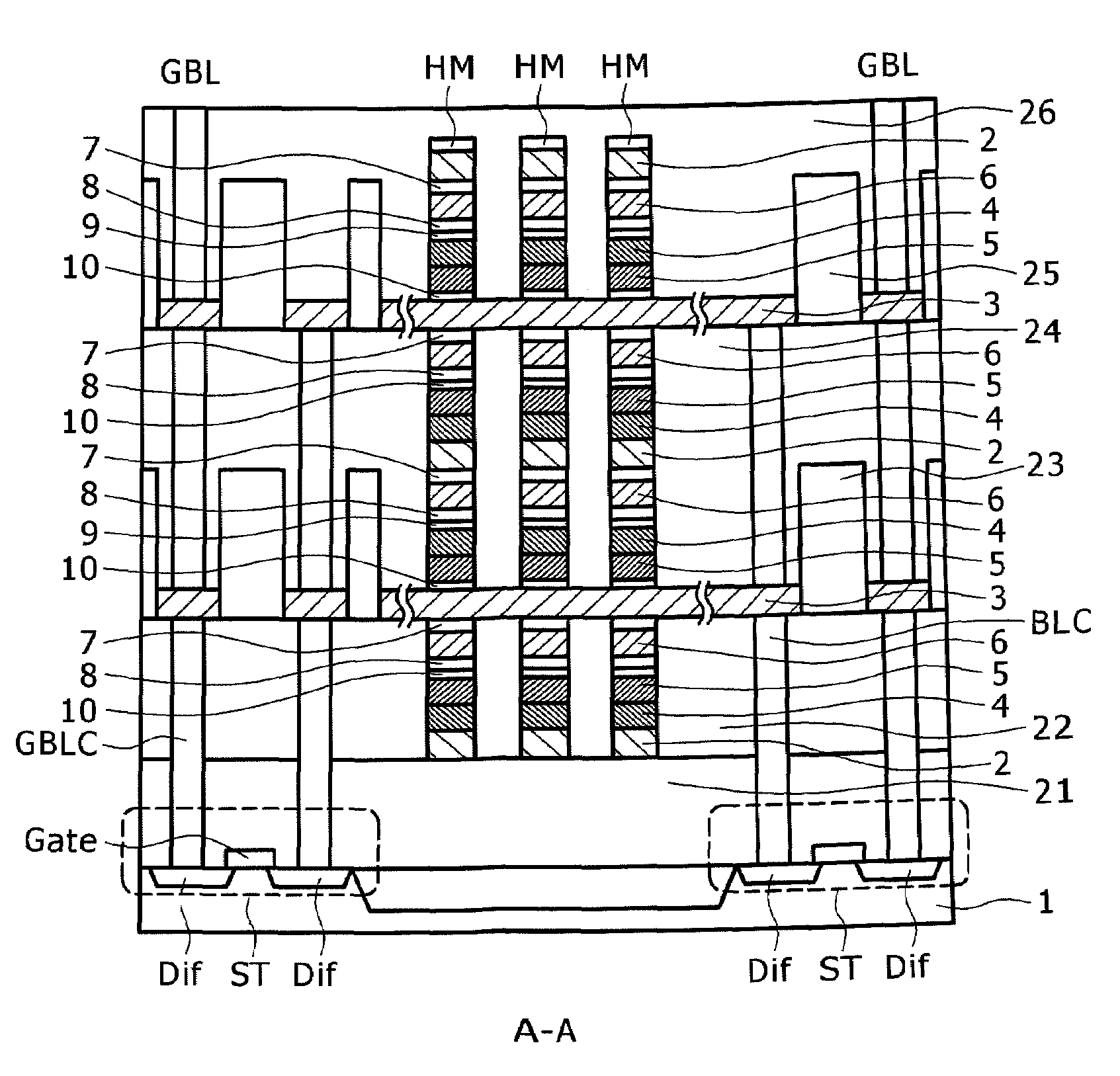
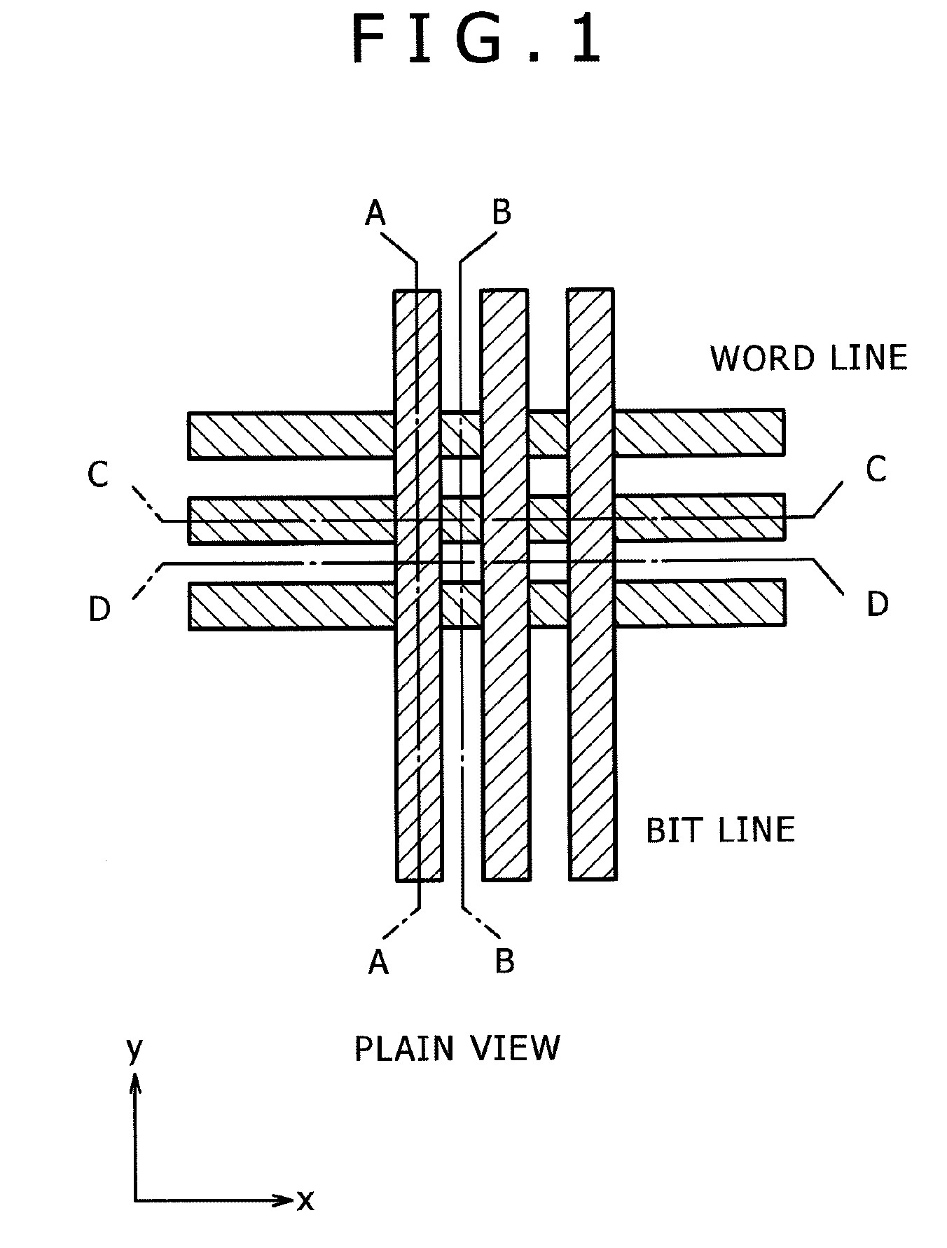
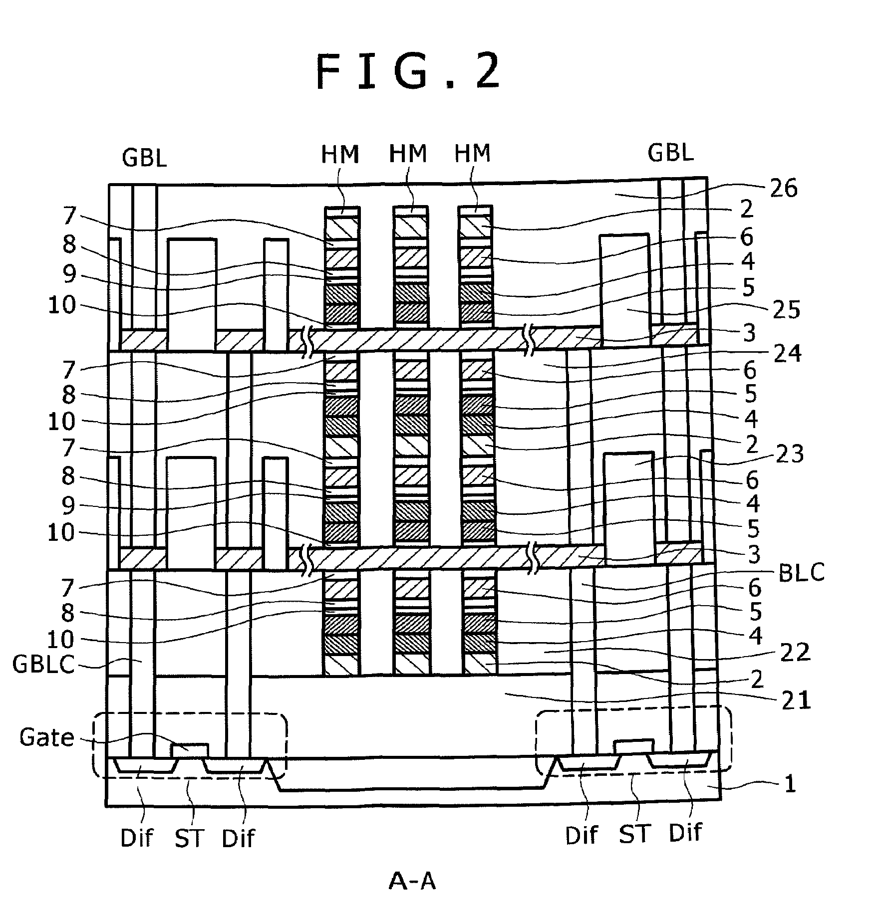
[0096]FIG. 1 is a partial plan view showing one example of a semiconductor memory device according to a first embodiment of the present invention and each of FIGS. 2 to 5 is a cross-sectional view taken along the line A-A, line B-B, line C-C, and line D-D in FIG. 1. Further, FIG. 6 is a cubic diagram showing a portion of a memory array. Moreover, in the plane view of FIG. 1 and the cubic diagram of FIG. 6, a portion of components is omitted to make the drawings easy to see.

[0097]The semiconductor memory device of the first embodiment uses a variable resistance element (for example, a phase change memory) as a memory element and a polysilicon diode as a selection device, wherein these form an array in a stacked cross point type. A word line extends in an X direction and a bit line extends in a y direction, inside a main plane of the semiconductor. Each line is connected to a diffusion layer of a selection transistor ST via a contact hole of an array end. The other diffusion layer of ...

second embodiment

[0132]In the first embodiment, when the crystallization of the amorphous silicon and the activation of the impurities are performed by laser annealing, the bit line material and the word line material just below the amorphous silicon covers the entire semiconductor main plane, while as described in a second embodiment, in performing laser annealing the manufacturing method that does not cover the entire semiconductor main plane with the word line material and the bit line material can be also permitted. FIGS. 37 to 46 show a method of manufacturing the semiconductor memory device according to the second embodiment.

[0133]First of all, like the first embodiment, the selection transistor and the peripheral circuit device are formed on the semiconductor substrate 1 and the insulating film 21 is formed thereon. Next, the word line material (for example, W) is deposited by the sputtering method. The deposition temperature of tungsten is 200° C. or less. Subsequently, the word line materia...

third embodiment

[0147]In the second embodiment, although the bit line material and the word line material are patterned and then, the amorphous silicon 14, 11, and 15, the silicides 9 and 10, the lower electrode 7, the phase change material 6, and the upper electrode 8 are deposited on the non-smoothed surface, as described in the third embodiment, a step caused in performing the lithography and the dry etching is small and the working can be easily performed, by performing the smoothness and then depositing the above-mentioned films. After performing the process of FIG. 37 of the second embodiment, the insulating film 31 is buried so that the word line 2 is completely buried and a portion of the insulating film 31 is removed by the CMP to expose the upper surface of the word line 2. Thereafter, through the process of the third embodiment, the semiconductor memory device is completed by performing the burying of the bit line and the word line by the insulating film and the smoothness of the surface...


PUM


Abstract

The present invention can promote the large capacity, high performance and high reliability of a semiconductor memory device by realizing high-performance of both the semiconductor device and a memory device when the semiconductor memory device is manufactured by stacking a memory device such as ReRAM or the phase change memory and the semiconductor device. After a polysilicon forming a selection device is deposited in an amorphous state at a low temperature, the crystallization of the polysilicon and the activation of impurities are briefly performed with heat treatment by laser annealing. When laser annealing is performed, the recording material located below the silicon subjected to the crystallization is completely covered with a metal film or with the metal film and an insulating film, thereby making it possible to suppress a temperature increase at the time of performing the annealing and to reduce the thermal load of the recording material.

Description

CLAIM OF PRIORITY[0001]The present application claims priority from Japanese patent application JP 2008-117055, filed on Apr. 28, 2008, the content of which is hereby incorporated by reference into this application.BACKGROUND OF THE INVENTION[0002]1. Field of the Invention[0003]The present invention relates to a semiconductor integrated circuit device and a method of manufacturing the same, and more particularly, to a technology that can realize high integration and high performance of an electrically rewritable nonvolatile semiconductor memory device.[0004]2. Description of the Related Art[0005]Among electrically rewritable nonvolatile semiconductor memory devices, a so-called flash memory, which can be batch erased, has been known. Recently, a demand for a flash memory as a memory device for small, portable information devices such as a portable personal computer, a digital still camera, and the like, has rapidly increased because it has excellent portability and high impact resis...

Claims


Application Information

Patent Timeline
IPC IPC(8): H01L47/00
CPCH01L21/02532H01L21/02675H01L27/2409H01L27/2481H01L45/146H01L45/06H01L45/1233H01L45/144H01L45/04H10B63/84H10B63/20H10N70/20H10N70/231H10N70/8828H10N70/8833H10N70/826
Inventor SASAGO, YOSHITAKATAKEMURA, RIICHIROKINOSHITA, MASAHARUMINE, TOSHIYUKISHIMA, AKIOMATSUOKA, HIDEYUKIHATANO, MUTSUKOTAKAURA, NORIKATSU
Owner HITACHI LTD
Why Eureka
Try Eureka