Apparatus and method for large area multi-layer atomic layer chemical vapor processing of thin films

a technology of atomic layer and thin film, which is applied in the direction of chemical vapor deposition coating, metal material coating process, coating, etc., can solve the problems of high quality and conformal thin film in narrow confinement, sub-micron geometrical features, and inability to deposit high quality and conformal thin films in narrow confinement, etc., to achieve the effect of facilitating the holding of substrate, high speed and high ra

Inactive Publication Date: 2009-12-10
GADGIL PRASAD
View PDF35 Cites 153 Cited by
  • Summary
  • Abstract
  • Description
  • Claims
  • Application Information

AI Technical Summary

Problems solved by technology

These and associated techniques of thin film deposition are flux dependent and thus can offer much desired thin film uniformity on larger area substrates with significant challenges in the apparatus design and its operation and at higher cost.
Although these techniques can deposit thin films at a high rate, ranging from several tens of nm / min to a few hundred nm / min., a glaring shortcoming is an inability to deposit high quality and conformal thin films in narrow, sub-micron geometrical features and film higher film thickness uniformity that is exceedingly difficult to achieve with increasing substrate area.
An ALD process, based on a well-known principle of chemisorption, forms a strongly adherent monolayer of reactive gas molecules, and is thus self limiting and also independent of the area of the substrate.
Moreover, an inert gas does not actively participate in the overall chemical reaction.
In practice a typical ALD process is quite slow as compared to a conventional CVD process because the ALD process critically depends on the time taken to complete one ALD process cycle.
As a result, practical application of ALD to large area substrates is restricted to very thin films—such as a few tens of nanometers or below.
However, batch processors are undesirable due to a variety of factors as substrate backside deposition, proportionately larger volume, and substrate load-unload time.
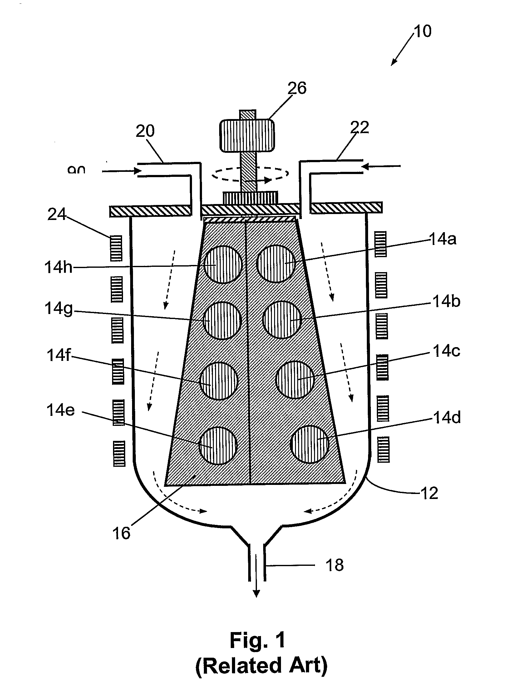
The barrel CVD reactor configuration, although useful on small-area substrates, however, is considered inefficient because of the internal gas flow mechanism, which is substantially parallel (longitudinal) to the substrate surface.
This flow configuration leads to longer path lengths and thus longer cycle time.
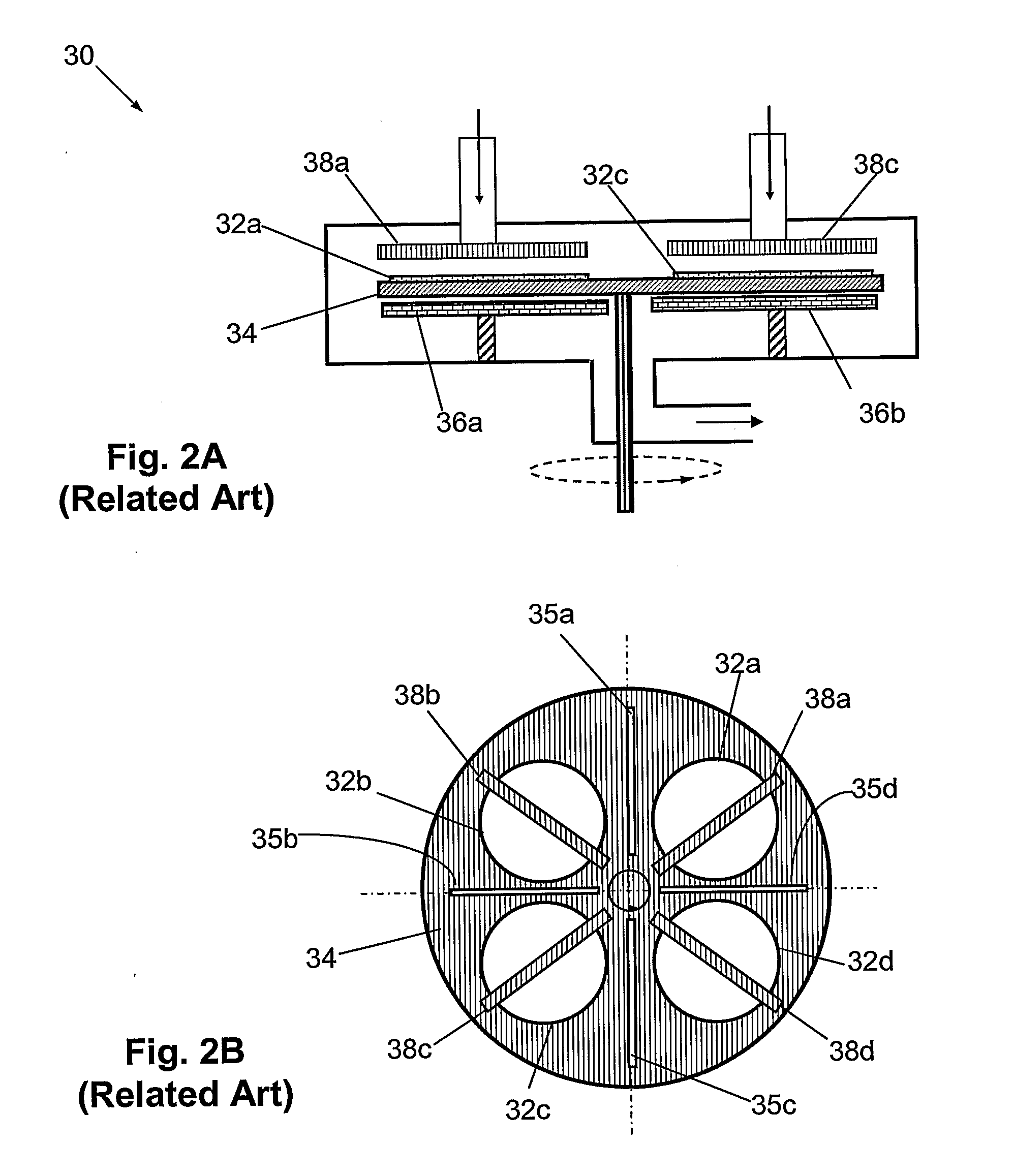
However, the gains that may be realized by multi-wafer ALD reactor configurations can be limited mainly because the reactor volume increases proportionately with the total area of the substrates, thus slowing the overall ALD cycle and the resultant deposition rate.
Also, time required to load and unload substrates, which adversely affects the effective throughput, needs to be taken into account.
Furthermore, the substrates such reactors can accommodate are often only planar.
The precursors employed for the ALD process were cuprous chloride (CuCl), indium trichloride (InCl3) and H2S and the substrates were glass, tin-oxide coated glass and nanoporous TiO2 coated glass with ALD process temperature in the range of 350-500° C. The rate of film deposition, however, at greater than 8 s / cycle, was rather slow for practical use to deposit about a micron thick absorber layer.
Such an ALD system, however, may have to contend with longer substrate load-unload times, inflexibility with respect to gas injection and substantially longer pulse width leading to longer cycle time—in the range of several minutes.
For a solar absorber layer about a micron thick, such a processing system may not entirely suitable.

Method used


Image

  • Apparatus and method for large area multi-layer atomic layer chemical vapor processing of thin films
  • Apparatus and method for large area multi-layer atomic layer chemical vapor processing of thin films
  • Apparatus and method for large area multi-layer atomic layer chemical vapor processing of thin films

Examples


example — 1

Example—1

Atomic Layer Deposition of Copper

[0101]Copper films can be deposited with one monolayer precision by employing cuprous halide with general formula CuX (X═F, Cl, Br and I) generated in-situ within the inner linear injector of the first composite nozzle, as described in the U.S. patent application Ser. No. 10 / 975,169; filed Oct. 27, 2004. The cuprous halide gas is subsequently combined with active hydrogen species (e.g., ionic species H+, free radicals H. and activated H2*) derived from H2 plasma. Alternately, CuX on the substrate surface can be combined with hydrogen free radicals (H.) obtained from a radical source connected to the inner linear injector of the second composite nozzle. For copper monolayer deposition process, the first and third composite nozzle each employs copper halide precursor while the second and fourth composite nozzles both employ species derived from hydrogen plasma or hydrogen free radicals to speed up the overall process.

[0102]The overall reaction...

example — 2

Example—2

Deposition of Copper Indium Diselenide Alloy Films

[0104]Thin films of Copper Indium Diselenide can be deposited in ALD mode by employing one of the precursors of copper as described in example−1 above, which is combined with the appropriate precursor of indium such as halide of indium e.g., indium trichloride [InCl3] which can be generated in-situ within the linear injector [ref. U.S. patent application Ser. No. 10 / 975,169 filed Oct. 27, 2004], tri-methyl indium [(CH3)3In], di-methly indium chloride [(CH3)2In—Cl], indium hexa-fluoro-pentanedionate [C15H3F18O6In] among others. The precursors of indium are not limited to the ones listed above. The preferred selenium precursor is H2Se gas which can be generated in-situ from solid selenium and hydrogen as described in the U.S. patent application Ser. No. 10 / 975,169 filed Oct. 27, 2004. The overall chemical reaction for synthesis of copper indium diselenide thin films can be given as (for sake of simplicity the reaction is shown...

example — 3

Example—3

Deposition of Copper Indium (Gallium) Selenide (CIGS) Graded Composition Films

[0106]Thin films of varying composition with thickness can be deposited in ALD mode by employing the ALCVP reactor configurations as described in FIGS. 17 and 18. The sources for copper and indium are as described, but are not limited to the ones, above. These can be combined with the appropriate gallium sources such as, but not limited to, tri-ethyl gallium [(CH3)3 Ga], diethyl-gallium chloride ((C2H5) Ga—Cl], and H2Se with N2 as the purge gas. During the ALD / CVD deposition process of Copper Indium (Gallium) Diselenide films, the flow of indium is increased that of gallium is proportionately decreased while maintaining the flow of H2Se. Such a process sequence in ALD or in CVD mode is of significant valve to develop graded optical gap, large area and high quality solar absorber materials in which the composition and optical band-gap of the material can be tuned with respect to the film thickness....


PUM

PropertyMeasurementUnit
acute angleaaaaaaaaaa
widthaaaaaaaaaa
thicknessaaaaaaaaaa

Abstract

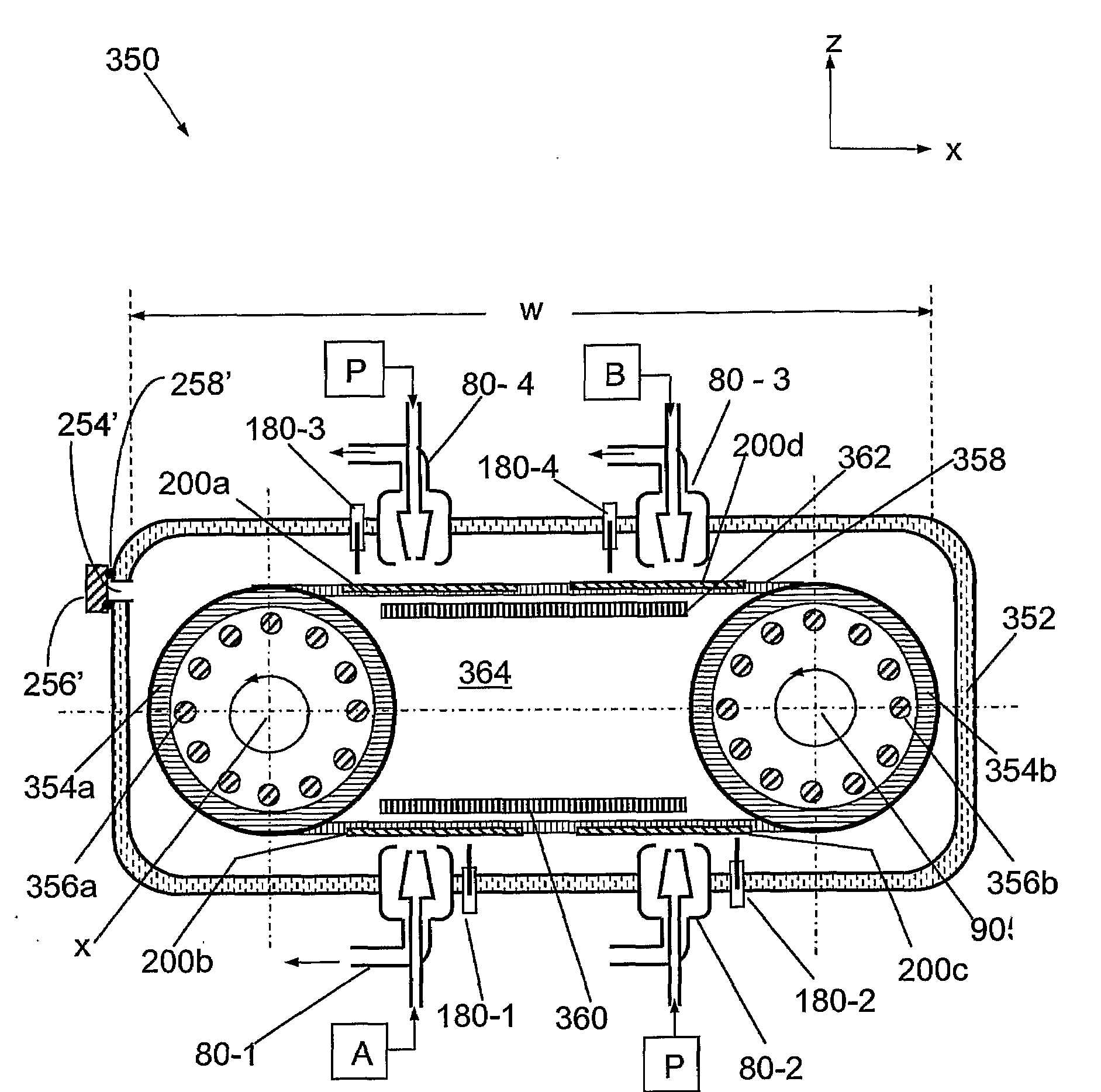
An apparatus and method for large area high speed atomic layer chemical vapor processing wherein continuous and alternating streams of reactive and inert gases are directed towards a co-axially mounted rotating cylindrical susceptor from a plurality of composite nozzles placed around the perimeter of the processing chamber. A flexible substrate is mounted on the cylindrical susceptor. In one embodiment, the process reactor has four composite injectors arranged substantially parallel to the axis of rotation of the cylindrical susceptor. In the other embodiment, the susceptor cross section is a polygon with a plurality of substrates mounted on its facets. The reactor can be operated to process multiple flexible or flat substrates with a single atomic layer precision as well as high-speed chemical vapor processing mode. The atomic layer chemical vapor processing system of the invention also has provisions to capture unused portion of injected reactive chemical precursors downstream.

Description

CROSS REFERENCE TO RELATED APPLICATION[0001]This application claims the benefit of the U.S. provisional application Ser. No. 60 / 656,772 filed Feb. 26, 2005 which is incorporated by reference herein.FIELD OF INVENTION[0002]The present invention is in the area of apparatus and methods for chemical vapor phase processing of multi-layer thin films of various materials at one atomic layer precision. More, particularly, this invention relates to processing of multi-layer thin films at one atomic layer precision on flexible substrates at high-speed for manufacturing of semiconductor devices, large area thin-film photovoltaic solar cells, flexible displays and catalytic electrodes for fuel cells, among other applications.BACKGROUND OF THE RELATED ART[0003]Thin film processing forms a critical part of fabrication of a variety of advanced devices such as microelectronic devices, optoelectronic and photonic devices, thin film photovoltaic solar cells and optical coatings and so on. In all thes...

Claims


Application Information

Patent Timeline
Patent Type & Authority Applications(United States)
IPC IPC(8): C23C16/44
CPCC23C16/4412C23C16/45525C23C16/45578C23C16/45551C23C16/45574C23C16/45531C23C16/305
Inventor GADGIL, PRASAD
Owner GADGIL PRASAD
Why Eureka
Try Eureka