[0013]
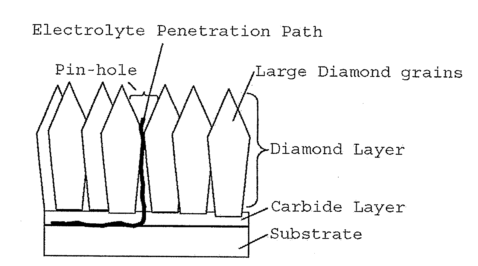
Diamond electrodes exhibits fascinating properties for example in removing COD component in
aqueous medium due to the huge amount of OH radical produced in its surface. Such performance can not be achieved by other conventional electrode such as
graphite electrode,
platinum or other
noble metal electrode like DSE (dimensionally stable electrode). Although diamond electrode performance being very promising; the industrial applicability has been strongly limited by its poor stability when used in almost all types of electrolytic reaction in
aqueous medium. Current DSE used in the Chloro-Alkali industry has stability longer than several years, but in comparison, the stability of actual diamond electrodes are extremely short. It is known by the status of art that when electrode with large diamond
layer thickness; for example higher than 50
micrometer is used, such
life time requirement can be cleared. Due to the difference in
thermal expansion coefficient, such high thickness diamond can be coated only in
silicon substrates. When
Niobium or other metals are used as the substrate, there is a bending of electrode due to the high temperature coating. Also there is a problem of remaining stress in the coating, which usually contributes to decrease the
life time of electrode. High thickness diamond coating are possible over the
silicon substrate, but the CVD coating cost of such large thickness diamond layer will become prohibitive for a commercial use. Therefore, the scope of present invention is to provide
a diamond electrode and a method for production of diamond electrode with lower production cost and improved stability.
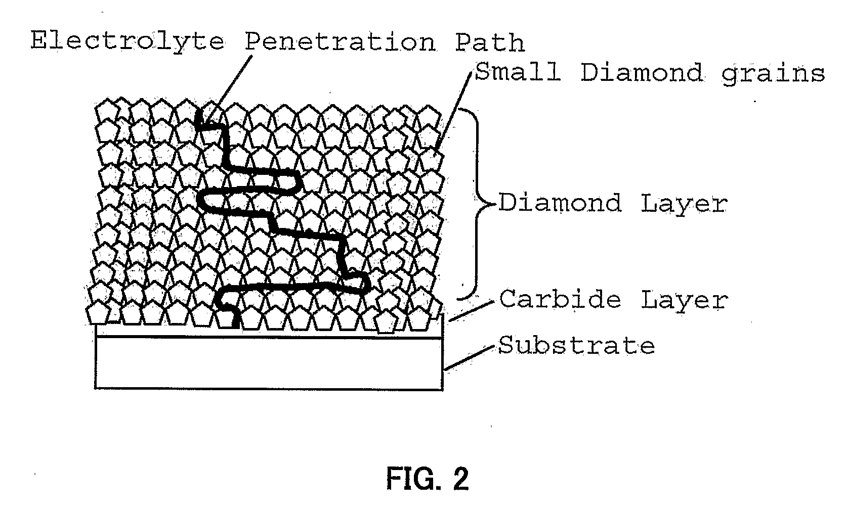
[0016]FIG. 2 shows a cross section of another embodiment of diamond electrode with different structure, which is one of preferred embodiment of present invention. In this embodiment of diamond electrode, the diamond layer is composed of small grains with size between 0.1-800 nm in width; preferable in the range between 1-500 nm; more preferable in the range between 1-300 nm. Because of the small grain size, the diamond layer is compact and has a minute structure which avoids the pinhole or cavity. This structure has the
advantage in blocking the penetration of electrolyte solution. Furthermore, even when the inter-granular region of the layer are etched and forms a path for the penetration of electrolyte solution through the diamond layer, this path is not a
straight path. Due to the small grain size, the path for the penetration of electrolyte solution becomes a labyrinthine path and this
path gain time until the electrolyte solution reaches to the
carbide interlayer. Then, such diamond electrode structure can clearly extend the life time and improve the stability of diamond electrode. Note that this diamond electrode is not a multilayer structure. This electrode is composed of single layer and basically homogeneous small grains of conductive diamond. Single structure layer have the
advantage that can be more easily produced in CVD coating than multilayer coatings. Multilayer structure requires change in the CVD parameter during the coating increasing the complexity of process. Also the meaning of homogeneous small grains used in this application do not means that the sizes of all grains are exactly the same. It means that the small grains with size between 0.1-800 nm in width; preferable in the range between 1-500 nm; more preferable in the range between 1-300 nm are dispersed homogenously in the layer.
[0025]Such features are essential to produce
a diamond electrode with improved stability.
[0026]Another embodiment of present invention is related to the method for producing the diamond electrode, in which the CVD coating is preceded by a pretreatment step. Such pretreatment step comprises the seeding of substrate with diamond nano
crystal. The seed diamonds are important to increase the growing rate of diamond layer during the CVD coating. If there are not any diamond crystals that can work as the nuclei to start the deposition of diamond carbons over the substrate, long coating time will be required. The seed diamond can be impregnated in the substrate by immersing the substrate in a solution containing seed diamond, water and some
solvent such as
methanol,
ethanol or
acetone. This impregnation of seed diamond is preferable done in a bath where there is an ultra-sonic treatment. The seed diamonds can not be higher than one
micrometer, by obvious reason, if this invention intents to provide a homogeneous layer composed of diamond grains lower than one micrometer. However, the seed diamonds are preferable lower than 200 nm, more preferable lower than 50 nm, further preferable lower than 5 nm. These nano seed crystals are necessary for providing many connection points between the substrate and the diamond layer in order to improve the cohesion of the coating. Furthermore the nano seed crystals reduce the
process time until a dense diamond layer is grown by the coalescence of the seed crystals.

