Lead-iodide-based scintillator materials

a technology of lead iodide and scintillator, which is applied in the direction of iodine oxygen compounds, halogen oxides/oxyacids, instruments, etc., can solve the problems of slow or low radiative efficiency, undoped semiconductors have rarely been used as scintillators, and achieves a higher signal-to-noise ratio, the effect of improving the signal-to-noise ratio of the tomographic image and reducing the dose dose dos

Inactive Publication Date: 2010-03-25
STC UNM
View PDF11 Cites 10 Cited by
  • Summary
  • Abstract
  • Description
  • Claims
  • Application Information

AI Technical Summary

Benefits of technology

[0008]The signal-to-noise ratio of a tomographic image can be improved through time-of-flight methods [Wong 1983]. High-brightness high-speed scintillators, such as LYSO [Muzic 2006], allow for extraction of very small, on the order of picoseconds, differences in scintillation times to provide a spread function along the detection volume containing the location of the annihilation events. This additional information leads to a higher signal to noise ratio, lower doses of radioactive tracers, faster imaging, and increased resolution of the reconstructed image [Wong 1983]. Fast and efficient scintillators are therefore crucial for time-of-flight PET applications.
[0009]Commonly used inorganic scintillators consist of a transparent insulator and an impurity functioning as a luminescence center. They are, in many cases, either slow or have low radiative efficiency. Indeed, in developing ultrafast scintillators, the luminescence via an intermediate excited state of an impurity is rather disadvantageous. Currently, the conventional cerium (Ce3+)-activated inorganic scintillators provide the best combination of speed and efficiency, but their radiative decay times are limited to ˜10-60 ns [van Loef 2001], [Weber 2002]. Direct excitonic luminescence from pure semiconductors could be employed by using the direct recombination of an electron and a hole with a decay time constant shorter than 10 ns. However, undoped semiconductors have rarely been used as scintillators, because of their poor luminescence efficiency at room temperature (RT). The excitonic level in a semiconductor is below the bottom of the conduction band by the binding energy Eb of the exciton. In bulk semiconductors, the excitonic level is not deep enough to prevent the thermal dissociation of excitons, and, as a result, the significant thermal quenching of excitonic luminescence at RT. Recently, very fast and efficient performance has been demonstrated from pure semiconducting scintillators such as PbI2 and HgI2 at cryogenic temperatures [Klintenberg 2002], [Derenzo 2002], [Klintenberg 2003]. Cooling the system to very low temperatures increased the population of excitons rather than free carriers by effectively suppressing the thermal perturbations, proportional to the thermal energy kBT.
[0010]Increasing the binding energy Eb of the exciton to the values exceeding the thermal energy kBT at RT (˜26 meV) is the requirement to thermally stabilize the excitonic level at RT. This can be realized by employing quantum confinement effect observed in low-dimensional quantum confinement systems (LD QCS). Enhancement of Coulomb

Problems solved by technology

They are, in many cases, either slow or have low radiative efficiency.
Indeed, in developing ultrafast scintillators, the luminescence via an intermediate excited state of an impurity is rather disadvantageous.
However, undoped semiconductors have rarely been used as scintillators, because of their poor luminescence efficiency at room temperature (RT).
In bulk semiconductors, the excitonic level is not deep enough to prevent the thermal dissociation of excitons, and, as a result, the significant thermal quenching of excitonic luminescence at RT.
Due to a poor match between QD emission at 540 nm and a PMT used to rec

Method used


Image

  • Lead-iodide-based scintillator materials
  • Lead-iodide-based scintillator materials
  • Lead-iodide-based scintillator materials

Examples


example 1

A. Synthesis of Lead-Iodide-Based Nanocrystals and Microcrystals

[0040]One synthesis procedure involves dissolution of bulk lead iodide in a coordinating solvent tetrahydrofuran (THF), subsequent re-crystallization with the addition of anhydrous methanol, and addition of dodecylamine (DDA) to obtain solvent-stabilized lead iodide NCs. The THF, anhydrous methanol, and DDA were purchased from Sigma Aldrich and used directly. A synthesis procedure also is described in [Finlayson, 2006], which was used for synthesis of PbI2 NCs.

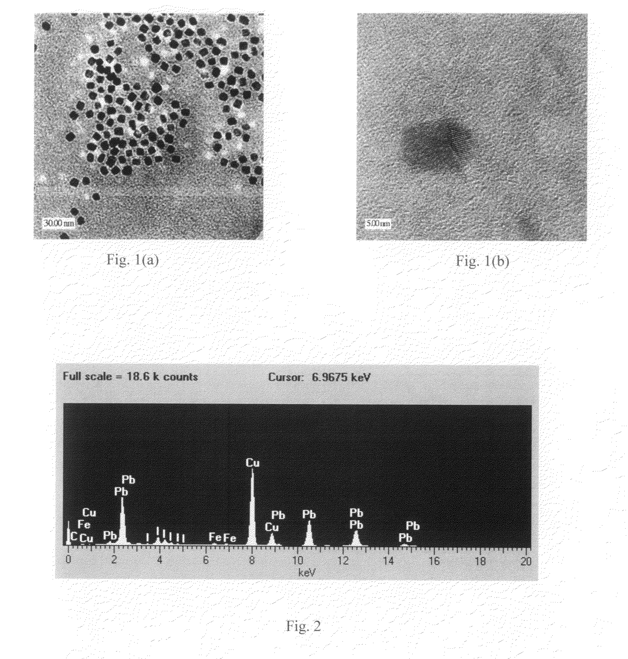
[0041]In a typical procedure, 100 mg of high purity (99.999%) lead (II) iodide powder is initially dissolved in 15 mL of THF under continuous stirring at RT (room temperature) and under atmospheric pressure. The above conditions are important, since solubility is a strong function of temperature and pressure. Subsequently, the solution is sonicated in centrifuge tubes in order to obtain a saturated solution. Then, to remove any insoluble suspension still present, ...

example 2

A. Second Synthesis of Lead-Iodide-Based Nanocrystals (PbIOH)

[0065]The synthesis procedure for PbIOH nanocrystals was a modification of PbClOH synthesis reported by H. Zhang, M. Zuo, G. Li, S. Tan and S. Zhang, “Laurionite nanowires and nanoribbons: rapid mechanochemical solution synthesis and optical properties”, Nanotechnology 16, pp. 3115-3119 (2005).

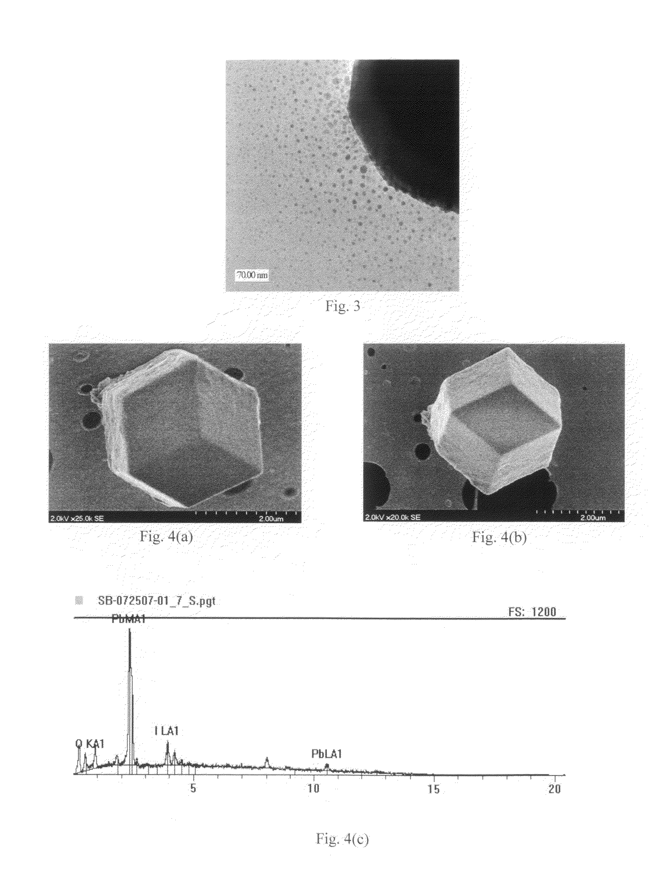
[0066]During a typical synthesis procedure, 0.461 g (˜1 mmol) of lead (II) iodide (PbI2) powder and 3 ml of 0.1 M sodium hydroxide (NaOH) solution were put into a mortar and ground with a pestle for 2 min at room temperature. The solution was collected and alternately centrifuged with deionized water, then centrifuged with ethanol, three times. The remaining yellowish samples were collected and stored in ethanol. An alternative method of synthesizing iodolaurionite was successfully accomplished by substituting potassium hydroxide (KOH) for the sodium hydroxide.

[0067]High-resolution TEM analysis revealed nanocrystals 3-15 nm in diamet...

example 3

A. Third Synthesis of Lead-Iodide-Based Nanocrystals (Pb3O2I2)

[0068]The synthesis procedure for Pb3O2I2 nanocrystals was a modification of Pb3O2Cl2 synthesis reported by K. Lozano, C. Hernandez, T. W. Petty, M. B. Sigman, B. Korgel, “Electrorheological analysis of nano laden suspensions”, Journal of Colloid and Interface Science 297, pp. 618-624 (2006).

[0069]In this synthesis, 0.332 g of high purity (99.999%) lead (II) iodide (PbI2) powder was added to 32 ml of deionized water. 25 ml of chloroform (CHCl3) with 0.17 g sodium octanoate (NaOOC(CH2)6CH3) were then added to the aqueous PbI2 solution forming two phases—an aqueous phase and a cloudy organic phase. The aqueous phase was then separated and discarded. 0.5 ml of ethylenediamine (C2H8N2) was added to the remaining organic solution. Evaporation of the organic solvent gave an opaque grayish-white solid, which served as the nanocrystal precursor. The precursor was heated in air for 60 min at 170° C. A dark grey solid was formed, a...


PUM


Abstract

Scintillator material comprising nanoparticles (nanocrystals) comprising lead (Pb), iodine (I), and optionally one or both of oxygen (O) and hydrogen (H) wherein the nanoparticles exhibit room-temperature scintillation under gamma irradiation. The scintillator nanoparticles can comprise Pb3O2I2. The scintillator nanoparticles can comprise PbIOH in generally equiatomic proportions or non-equiatomic variants thereof that exhibit scintillation under gamma irradiation. The scintillator nanoparticles have a particle dimension in the range of about 5 to about 100 nm. Microparticles (microcrystals) also are provided comprising lead (Pb), iodine (I), and optionally one or both of oxygen (O) and hydrogen (H) grown in a nanoparticle colloidal solution over time to a particle dimension greater than 0.1 μm, such as about 2 microns.

Description

[0001]This application claims benefits and priority of provisional application Ser. No. 61 / 072,636 filed Mar. 31, 2008, the disclosure of which is incorporated herein by reference.CONTRACTUAL ORIGIN OF THE INVENTION[0002]The invention was with government support under National Science Foundation under Grants IIS-0610201 and CBET-0736241 awarded by the National Science Foundation. The government has rights in the invention.FIELD OF THE INVENTION[0003]The present invention relates to a scintillator material comprising a lead-iodide-based material in a nanoparticle or microparticle morphology wherein the scintillator material exhibits scintillation when exposed to gamma irradiation.BACKGROUND OF THE INVENTION[0004]Semiconductor nanocrystals (NCs) or quantum dots (QDs) have been extensively investigated over the last decade for a variety of biomedical, biochemical sensing, and optoelectronic applications. An area that has received relatively little attention so far is the use of NCs as ...

Claims


Application Information

Patent Timeline
IPC IPC(8): G01T1/20C01B11/22
CPCC01B9/06C01G21/00C01P2002/72C01P2002/82G01T1/2023C01P2004/04C01P2004/62C01P2006/10C01P2004/03
Inventor OSINSKI, MAREK A.WITHERS, NATHAN J.AKINS, BRIAN A.SMOLYAKOV, GENNADY A.SANKAR, KRISHNAPRASAD
Owner STC UNM
Why Eureka
Try Eureka