

Film for manufacturing semiconductor device and method of manufacturing the same
a technology for semiconductor devices and films, applied in the direction of chemistry apparatus and processes, transportation and packaging, other domestic articles, etc., can solve the problem of film floating phenomenon of cover films, and achieve the effects of facilitating semiconductor chip recovery, reducing yield, and excellent shape stability of die-bonding films
- Summary
- Abstract
- Description
- Claims
- Application Information
AI Technical Summary
Benefits of technology
Problems solved by technology
Method used
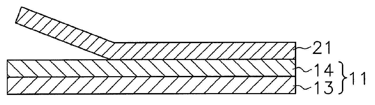
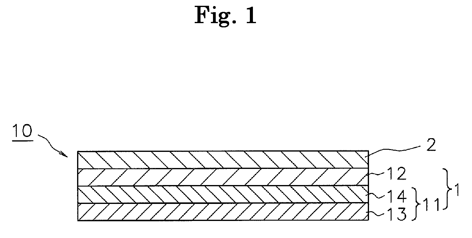
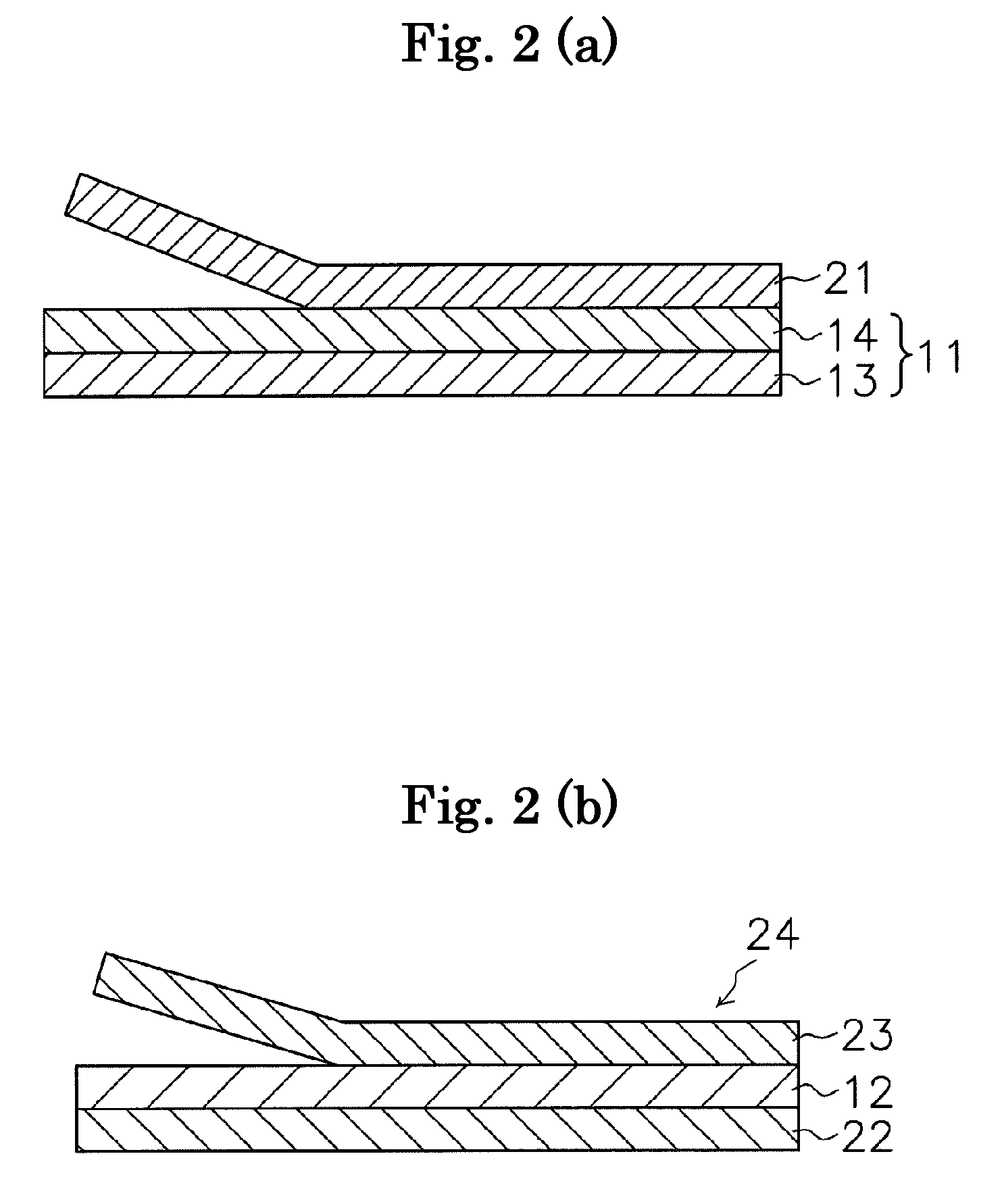
Image

Examples
example 1
[0097]
[0098]Acrylic polymer A having a weight average molecular weight of 850,000 was obtained by placing 88.8 parts of 2-ethylhexyl acrylate (below, referred to as “2EHA”), 11.2 parts of 2-hydroxyethyl acrylate (below, referred to as “HEA”), 0.2 part of benzoyl peroxide, and 65 parts of toluene in a reactor equipped with a cooling tube, a nitrogen-introducing tube, a thermometer, and a stirring apparatus, and performing a polymerization treatment at 61° C. in a nitrogen airflow for 6 hours. The molar ratio of 2EHA and HEA was made to be 100 mol: 20 mol. The weight average molecular weight is described later.
[0099]Acrylic polymer A′ was obtained by adding 12 parts (80 mol % to HEA) of 2-methacryloyloxyehyl isocyanate (below, referred to as “MOI”) into this acrylic polymer A and performing an addition reaction treatment at 50° C. in an air flow for 48 hours.
[0100]Next, a pressure-sensitive adhesive solution was produced by adding 8 parts of an isocyanate crosslinking agent (trade nam...
example 2
[0124]
[0125]The same dicing film in Example 1 was used as the dicing film according to the present example.
[0126]
[0127]2 parts of an isocyanate crosslinking agent (trade name “CORONATE HX” manufactured by Nippon Polyurethane Industry Co., Ltd.), 35 parts of an epoxy resin (trade name “EPICOAT 1001” manufactured by Japan Epoxy Resins Co., Ltd.), 37 parts of a phenol resin (trade name “MILEX XLC-4L” manufactured by Mitsui Chemicals, Inc.), and 30 parts of spherical silica (trade name “SO-25R”, average particle size of 0.5 μm, manufactured by Admatechs) as an inorganic filler to 100 parts of an ester acrylate polymer (trade name “PARACRON W-197CM”, Tg: 18° C., manufactured by Negami Chemical Industrial Co., Ltd.) having ethyl acrylate-methyl methacrylate as a main component were dissolved into methylethylketone, and it was prepared so that the concentration became 21.4% by weight.
[0128]A coated layer was formed by applying the solution of this pressure-sensitive adhesive composition on...
reference example 1
[0144]
[0145]The same dicing film in Example 1 was used as the dicing film according to the present reference example.
[0146]
[0147]The dicing film according to the present reference example was produced in the same manner as Example 1 except that the added amount of the inorganic filler was changed to 95 parts.
[0148]
[0149]The dicing die-bonding film according to the present reference example was produced in the same manner as Example 1.
[0150](Method of Measuring the Tensile Modulus of the Pressure-Sensitive Adhesive Layer)
[0151]A sample having a length of 10.0 mm, a width of 2 mm, and a cross section of 0.1 to 0.5 mm2 was cut out from the dicing film of each of the Examples and Comparative Examples. The tensile test was performed on this sample in the MD in a condition of measurement temperature 23° C., distance to a chuck 50 mm, and tensile speed 50 mm / min, and the changing length (mm) of the sample that was due to the sample being stretched was measured. A value was made to be the t...
PUM
| Property | Measurement | Unit |
|---|---|---|
| temperature | aaaaa | aaaaa |
| tensile storage modulus | aaaaa | aaaaa |
| glass transition temperature | aaaaa | aaaaa |
Abstract
Description
Claims
Application Information