
Multiple quantum dot waveguides

a quantum dot waveguide and quantum dot technology, applied in the field of multi-quantum dot waveguides, can solve the problems of preventing the manufacture of ultra-high density photonic circuits, difficult integration and packaging dimensions, and easy guide light, so as to reduce propagation loss, enhance the use and versatility, and design flexibility

Inactive Publication Date: 2010-09-02
UNIV OF WASHINGTON
View PDF3 Cites 2 Cited by
  • Summary
  • Abstract
  • Description
  • Claims
  • Application Information

AI Technical Summary

Benefits of technology

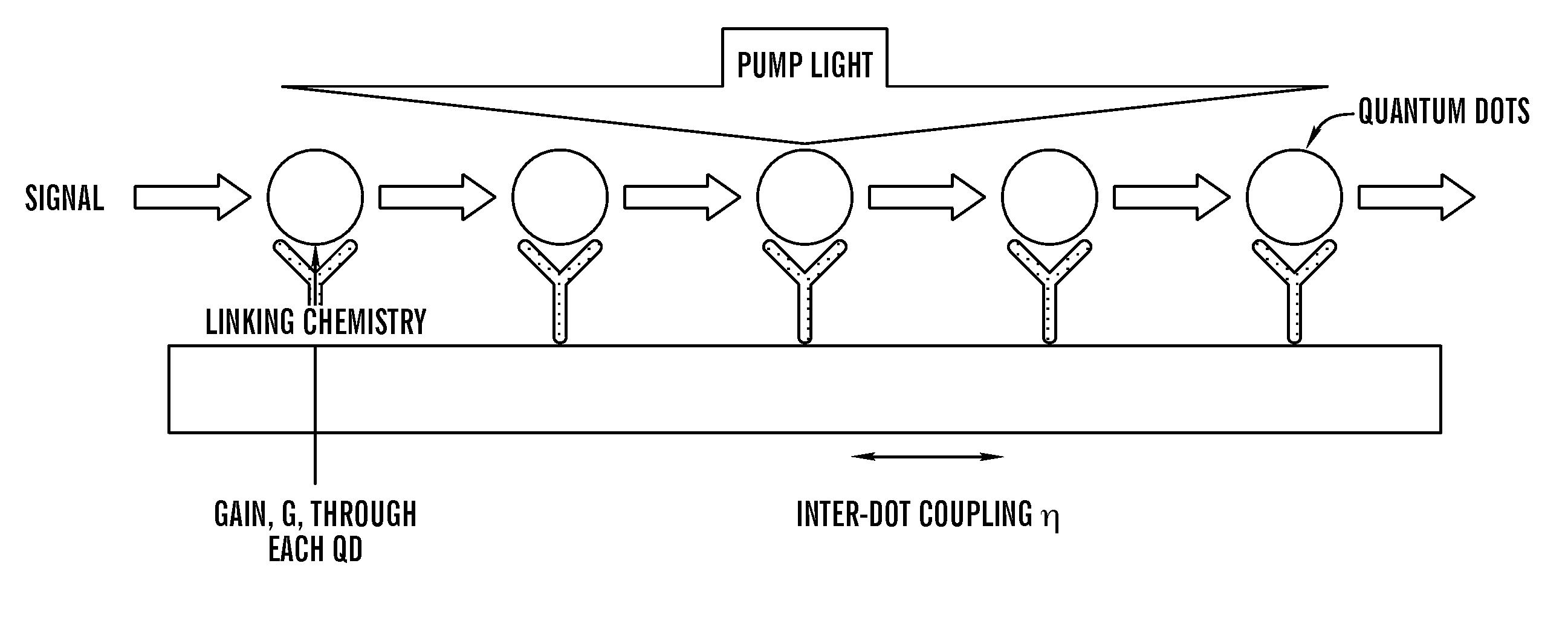
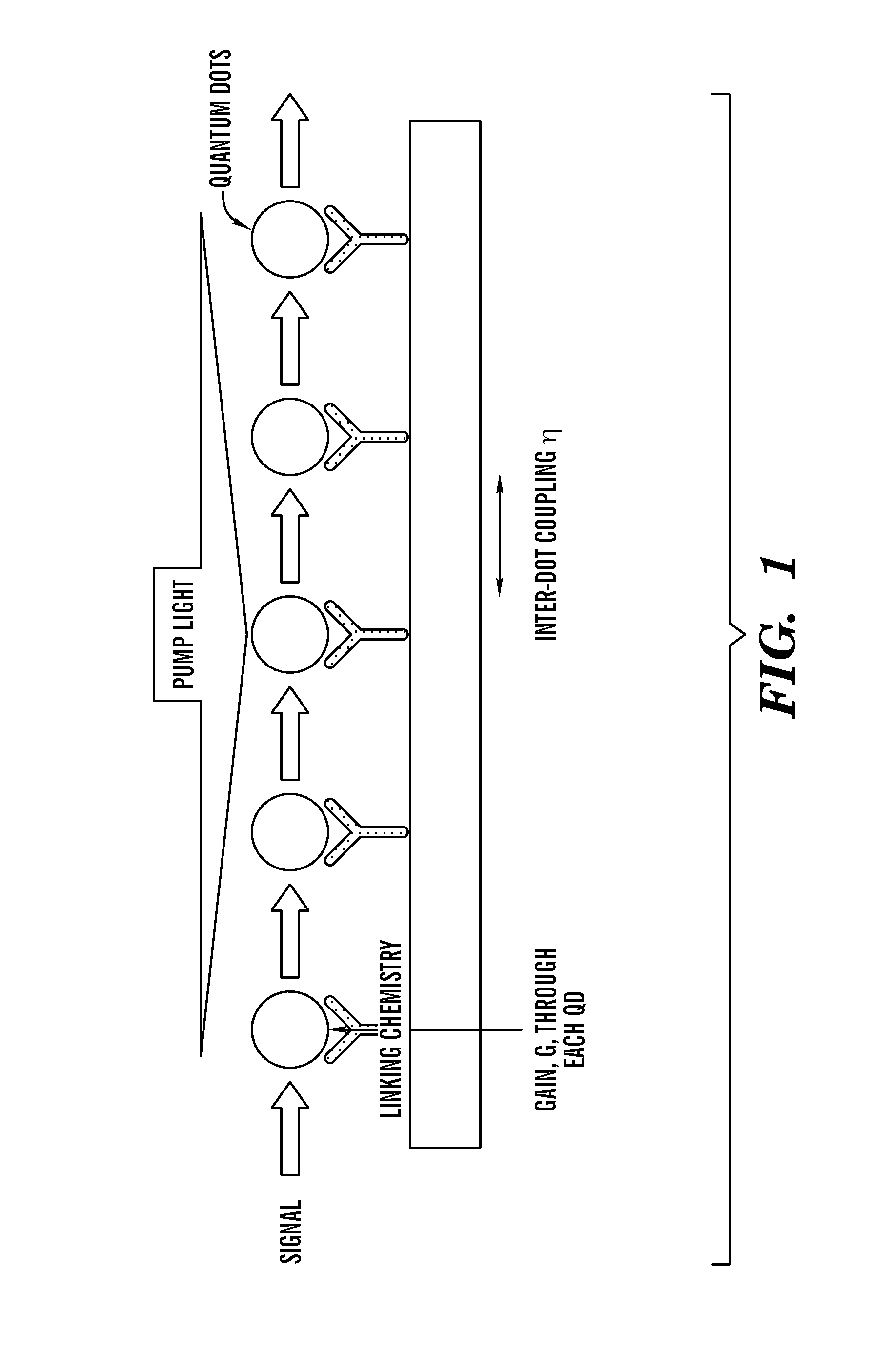
[0007]The use of quantum dots, a semiconducting nanoparticle, to form waveguides allows for self-assembly by chemical bonding, reduction of propagation loss, and flexibility in design since electrical and optical signals are both appropriate means of excitation. For the first point, conjugating QDs to molecules with selective chemistry and terminal linkers produces specific attachment schemes that enhance its use and versatility. As for the latter two advantages, the gain mechanism hinges on operation by a pump source to create population inversion of excited electrons to generate net emission over absorption, similar to optical amplifying action. Indeed, the process has been proven over the past decade, where QD lasers have been successfully demonstrated with lower threshold current density compared to those made from bulk material with sharp emission peaks due to the three-dimensional quantum confinement nature of the particle (Ledentsov et al.,IEEE J. Select. Topics Quantum Electron. 6:439 (2000); Ustinov et al., Quantum Dot Lasers; Oxford University Press: Oxford, (2003); and Asada et al., IEEE J. Quantum Electron. 22:1915 (1986)). Consequently, the propagating wave may not only experience less transmission loss but an increase in strength as well. In view of the unique advantages of quantum dots, they are highly suitable for use as new nano-scale photonic waveguide structure.

Problems solved by technology

Currently, the inability to easily guide light at sub-diffraction limit dimensions prevents the manufacture of ultra-high density photonic circuits.
23:401 (2005)) waveguides enable nanoscale signal transmission, challenges with integration and packaging dimensions remain.
Still, negative dielectrics, such as metals, are subject to resistive heating and loss, and require conversion to translate plasmonic to optical energy.

Method used


Image

  • Multiple quantum dot waveguides
  • Multiple quantum dot waveguides
  • Multiple quantum dot waveguides

Examples


example 1

Evaluation of Gain Per Quantum Dot

[0048]Prior modeling of the gain response for 5 nm×5 nm×5 nm CdSe / ZnS core / shell quantum dots indicates that there is net emission occurring between 0.1 and 1 nW optical pump power, with absorption dominating at the low end and gain saturation at the higher end (Wang et al., IEEE J. of Select. Topics in Quantum Electron. 11:500 (2005), which is hereby incorporated by reference in its entirety). Furthermore, implementing an ABCD transfer matrix technique allows estimation of the relative output intensity with respect to coupling coefficient between two QDs and the gain parameter inherent in each. The results show a tradeoff between gain and coupling where a smaller value for one may compensate a higher value for the other to attain high transmission efficiency. FIG. 6 depicts the simulation result of transmission efficiency for a waveguide composed of a five QD 1D-array waveguide.

example 2

Evaluation of Layer Deposition

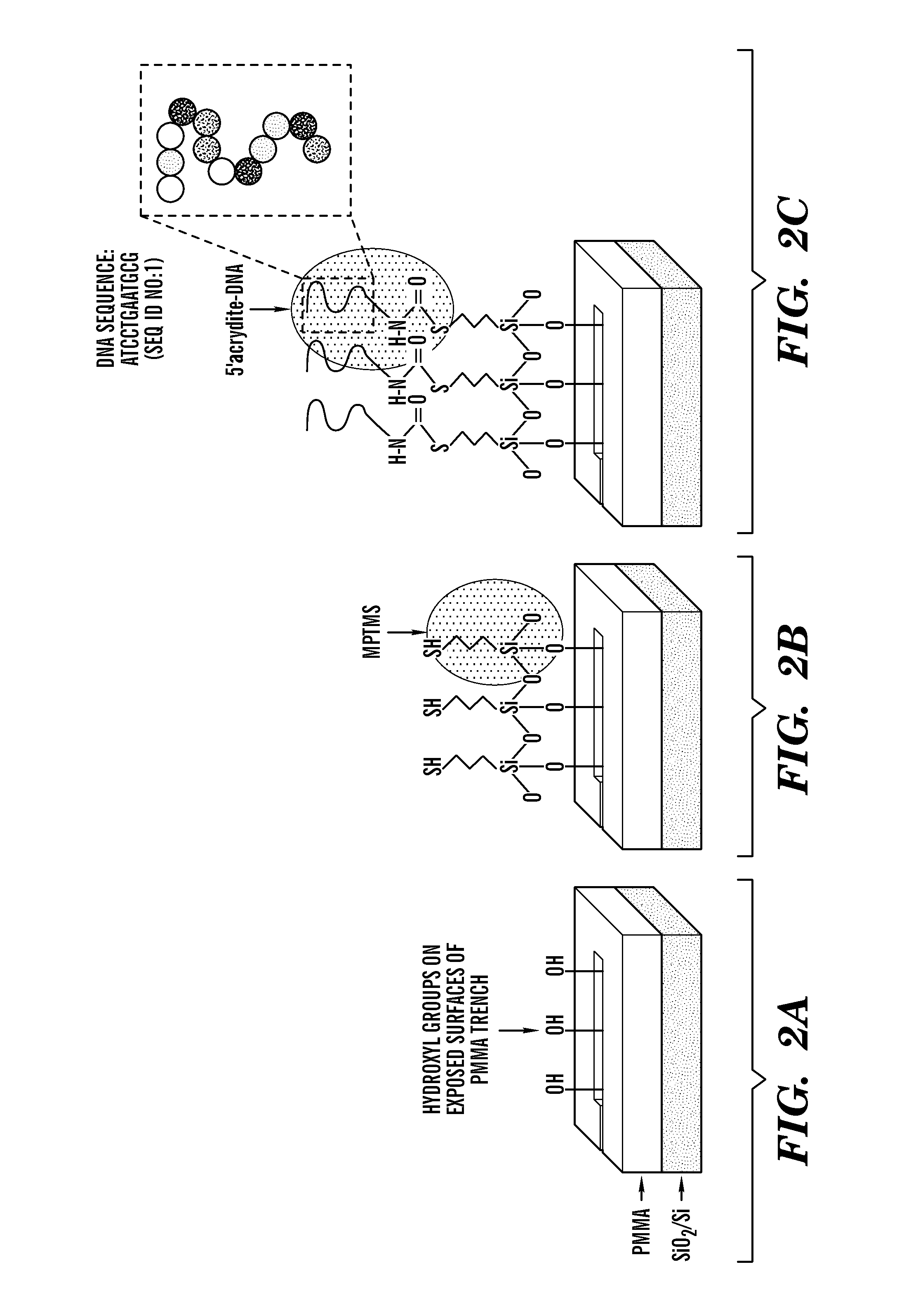
[0049]To provide an element of selectively, single-stranded DNA (ss-DNA) and its complementary chain (cDNA) are used to program the binding of nanocrystals to the substrate and present a means for depositing an array of structures tailored to operate at different wavelengths. The procedure (shown in FIG. 2) to build a sub-diffraction limit waveguide begins with cleaving a small coupon, generally 1 cm×1 cm area, from an oxidized silicon wafer. The sample is cleaned by rinsing with xylene, acetone, isopropyl alcohol (IPA), and de-ionized (DI) water followed by drying with nitrogen gas, N2 (Ramanath et al., “Self-assembled Subnanolayers as Interfacial Adhesion Enhancers and Diffusion Barriers for Integrated Circuits,”Appl. Phys. Lett. 83(2):383-385 (2003), which is hereby incorporated by reference in its entirety). Then, the sample is spin-coated with polymethylmethacrylate (PMMA), which acts as a positive resist and soft baked on a hot plate before placin...

example 3

Evaluation of Layer Deposition

[0052]To check the deposition of the self-assembled molecular (SAM) layers, samples that underwent the assembly processes to control samples using x-ray photoelectron spectroscopy (XPS) were compared. The MPTMS results in FIG. 8A, which provide the percent composition of the elements in the top 10 nm of the surface, show sulfur content only for devices subjected to the deposition step. The peaks are labeled for the compounds of interest and the average % composition are found to be 48.9% oxygen, 25.7% silicon, 24.3% carbon, and 1.1% sulfur, reflecting the existence of the silicon dioxide substrate, inevitable carbon contamination, and MPTMS molecules. Further assembly steps using DNA are confirmed with fluorescence observation and examples of the final QD fluorescence patterns, in

[0053]FIG. 8B, include an array of rectangles ranging in size from 5 μm×1 μm to 1 μm×1 μm, and a 1 μm wide waveguide.

[0054]All formations including the smallest at 1 μm2 are we...


PUM


Abstract

The present invention relates to an assembly of multiple waveguides which includes a substrate and a plurality of waveguides positioned on said substrate at locations effective to suppress cross-talk between different waveguides. The plurality of waveguides each comprise an elongate array of quantum dots extending between sets of first and second locations on the substrate. The waveguides are positioned to receive: (1) pumped light uniformly applied to the array to produce electron-hole pairs and to enable optical gain and (2) signal light at the first location to trigger an emission from the quantum dot at the first location and transmission of photons along the array to the second location. A light transmission system which includes this assembly as well as methods of making and using the assembly are also disclosed.

Description

[0001]This application is a continuation of U.S. patent application Ser. No. 11 / 750,787, filed May 18, 2007, which claims priority benefit of U.S. Provisional Patent Application Ser. No. 60 / 802,177, filed May 19, 2006, which are hereby incorporated by reference in their entirety.FIELD OF THE INVENTION[0002]The present invention is directed to multiple quantum dot waveguides, methods of making and using these waveguides, as well as light transmission systems.BACKGROUND OF THE INVENTION[0003]Currently, the inability to easily guide light at sub-diffraction limit dimensions prevents the manufacture of ultra-high density photonic circuits. To capture the inherent advantages of large bandwidth, capacity, and high speed modulation, research in the area has been underway for over a decade. While a number of proposed structures like the one-dimensional negative dielectric (Takahara et al., Optics Lett. 22:475 (1997)) and silicon-on-insulator photonic crystal (Bogaerts et al., IEEE J. of Lig...

Claims


Application Information

Patent Timeline
Patent Type & Authority Applications(United States)
IPC IPC(8): G02B6/00H04B10/12H05K3/00G02B6/10
CPCB82Y20/00G02B6/1221H01S5/021H01S5/041Y10T29/49124H01S5/4025H01S5/50H01S5/5027H01S5/3412
Inventor LIN, LIH Y.WANG, CHIA-JEANPARVIS, BABAK A.
Owner UNIV OF WASHINGTON
Learn More