

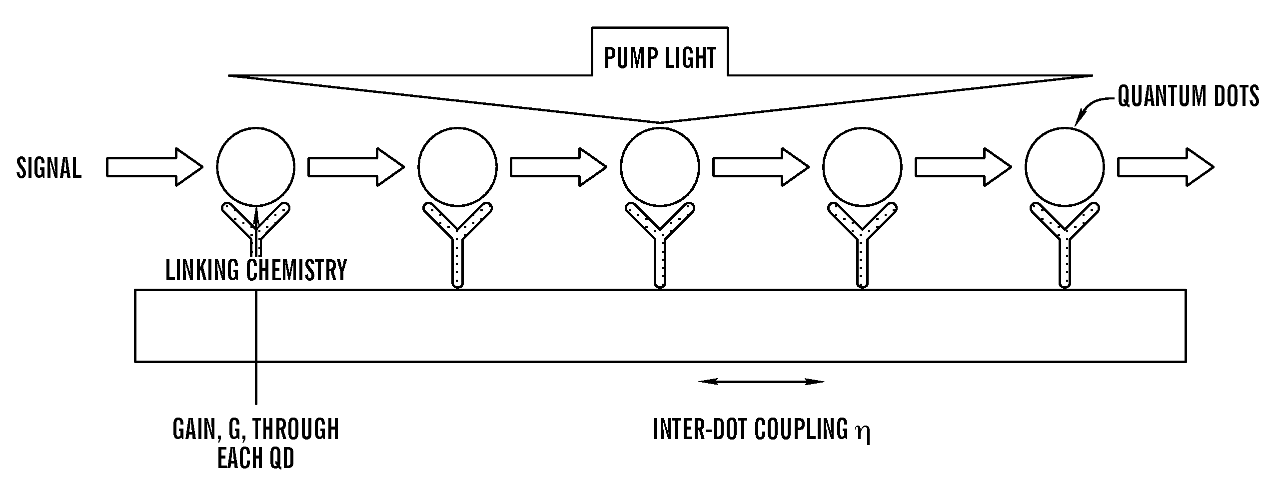
Multiple quantum dot waveguides
a quantum dot waveguide and quantum dot technology, applied in the field of multi-quantum dot waveguides, can solve the problems of preventing the manufacture of ultra-high density photonic circuits, difficult integration and packaging dimensions, and easy guide light, so as to reduce propagation loss, enhance the use and versatility, and design flexibility
- Summary
- Abstract
- Description
- Claims
- Application Information
AI Technical Summary
Benefits of technology
Problems solved by technology
Method used
Image

Examples
example 1
Evaluation of Gain Per Quantum Dot
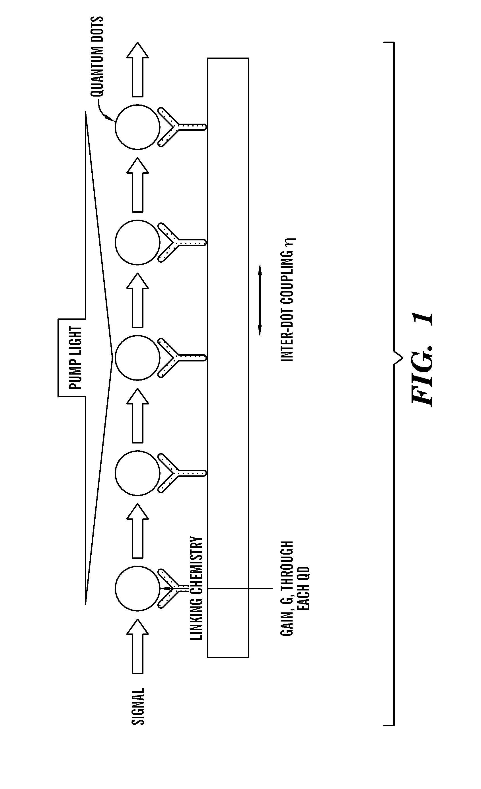
[0048] Prior modeling of the gain response for 5 nm×5 nm×5 nm CdSe / ZnS core / shell quantum dots indicates that there is net emission occurring between 0.1 and 1 nW optical pump power, with absorption dominating at the low end and gain saturation at the higher end (Wang et al., IEEE J. of Select. Topics in Quantum Electron. 11:500 (2005), which is hereby incorporated by reference in its entirety). Furthermore, implementing an ABCD transfer matrix technique allows estimation of the relative output intensity with respect to coupling coefficient between two QDs and the gain parameter inherent in each. The results show a tradeoff between gain and coupling where a smaller value for one may compensate a higher value for the other to attain high transmission efficiency. FIG. 6 depicts the simulation result of transmission efficiency for a waveguide composed of a five QD 1D-array waveguide.
example 2
Evaluation of Layer Deposition
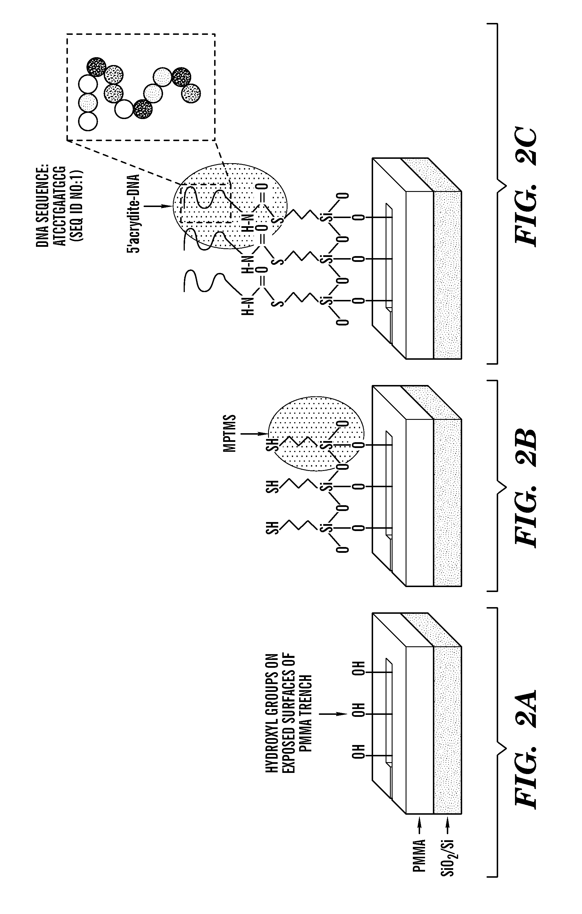
[0049] To provide an element of selectively, single-stranded DNA (ss-DNA) and its complementary chain (cDNA) are used to program the binding of nanocrystals to the substrate and present a means for depositing an array of structures tailored to operate at different wavelengths. The procedure (shown in FIG. 2) to build a sub-diffraction limit waveguide begins with cleaving a small coupon, generally 1 cm×1 cm area, from an oxidized silicon wafer. The sample is cleaned by rinsing with xylene, acetone, isopropyl alcohol (IPA), and de-ionized (DI) water followed by drying with nitrogen gas, N2 (Ramanath et al., “Self-assembled Subnanolayers as Interfacial Adhesion Enhancers and Diffusion Barriers for Integrated Circuits,”Appl. Phys. Lett. 83(2):383-385 (2003), which is hereby incorporated by reference in its entirety). Then, the sample is spin-coated with polymethylmethacrylate (PMMA), which acts as a positive resist and soft baked on a hot plate before plac...
example 3
Evaluation of Layer Deposition
[0052] To check the deposition of the self-assembled molecular (SAM) layers, samples that underwent the assembly processes to control samples using x-ray photoelectron spectroscopy (XPS) were compared. The MPTMS results in FIG. 8A, which provide the percent composition of the elements in the top 10 nm of the surface, show sulfur content only for devices subjected to the deposition step. The peaks are labeled for the compounds of interest and the average % composition are found to be 48.9% oxygen, 25.7% silicon, 24.3% carbon, and 1.1% sulfur, reflecting the existence of the silicon dioxide substrate, inevitable carbon contamination, and MPTMS molecules. Further assembly steps using DNA are confirmed with fluorescence observation and examples of the final QD fluorescence patterns, in FIG. 8B, include an array of rectangles ranging in size from 5 μm×1 μm to 1 μm×1 μm, and a 1 μm wide waveguide.
[0053] All formations including the smallest at 1 μm2 are wel...
PUM
| Property | Measurement | Unit |
|---|---|---|
| width | aaaaa | aaaaa |
| width | aaaaa | aaaaa |
| width | aaaaa | aaaaa |
Abstract
Description
Claims
Application Information